Semiconductor structure and forming method thereof

A semiconductor, volume ratio technology, applied in semiconductor devices, semiconductor/solid-state device manufacturing, semiconductor/solid-state device components, etc., can solve the problem that the etching process needs to be improved

Pending Publication Date: 2020-12-29
SEMICON MFG INT (SHANGHAI) CORP +1
View PDF0 Cites 0 Cited by
  • Summary
  • Abstract
  • Description
  • Claims
  • Application Information

AI Technical Summary

Problems solved by technology

[0004] However, the existing etc...

Method used


Image

  • Semiconductor structure and forming method thereof
  • Semiconductor structure and forming method thereof
  • Semiconductor structure and forming method thereof

Examples


Embodiment Construction

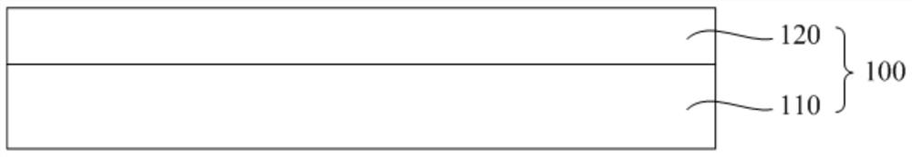
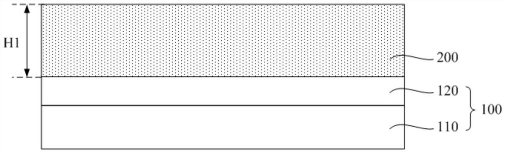
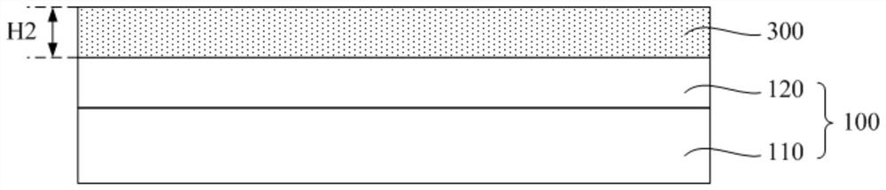
[0019] A method for forming a semiconductor structure is now analyzed, including: providing a substrate (not shown in the figure); forming a polysilicon film (not shown in the figure) on the substrate; performing oxidation treatment on a partial thickness of the polysilicon film to form The silicon oxide layer, the remaining thickness of the polysilicon film is used as the polysilicon layer; the silicon oxide layer is removed by etching.

[0020] The oxidation treatment process and the etching process are carried out in steps, so that the process efficiency is low. In addition, the difficulty of process control is increased, which affects the formation quality of the polysilicon layer.

[0021] The inventor has conducted research on the formation method of the above-mentioned semiconductor structure, and through creative work, the inventor has noticed that the partial thickness polysilicon film can be etched by etching with a mixture of hydrofluoric acid and ozone solution. By...


PUM


Abstract

The invention discloses a semiconductor structure and a forming method thereof. The forming method comprises steps of providing a substrate; forming a polycrystalline silicon film on the substrate; and removing a part of the polycrystalline silicon film by adopting an etching process to form a polycrystalline silicon layer, the etching solution being a mixed solution of hydrofluoric acid and an ozone solution, and the volume ratio of the hydrofluoric acid to the ozone solution being 1: 4-4: 1. According to the method, etching precision can be improved, and flatness of the surface of the polycrystalline silicon layer can be improved.

Description

technical field [0001] The invention relates to the technical field of semiconductor manufacturing, in particular to a semiconductor structure and a forming method thereof. Background technique [0002] Polysilicon is a form of elemental silicon. When molten elemental silicon is solidified under supercooled conditions, silicon atoms are arranged in the form of diamond lattices to form many crystal nuclei, and these crystal nuclei grow into crystal grains with different crystal plane orientations, and these crystal grains combine to crystallize into polycrystalline silicon. [0003] Polysilicon materials may be used to form hard mask layers or masking layers in the fabrication process of semiconductor structures. In order to make the thickness of the formed polysilicon layer meet the process requirements, the polysilicon material needs to be etched. [0004] However, the existing etching process still needs to be improved. Contents of the invention [0005] The problem t...

Claims


Application Information

Patent Timeline
IPC IPC(8): H01L21/306H01L21/033H01L21/56H01L23/29H01L23/31
CPCH01L21/0337H01L21/30604H01L21/56H01L23/298H01L23/3171
Inventor 潘璋
Owner SEMICON MFG INT (SHANGHAI) CORP
Why Eureka
Try Eureka