Micro-ring coupling modulation structure based on graphene fine tuning coupling efficiency and use method thereof

A technology of coupling efficiency and coupling structure, applied in the field of optoelectronics, can solve the problems of limited, non-tunable, and inability of micro-ring coupling efficiency, and achieve the effect of reduced process tolerance requirements and high precision

Inactive Publication Date: 2021-01-01
UNIV OF ELECTRONIC SCI & TECH OF CHINA
View PDF5 Cites 3 Cited by
  • Summary
  • Abstract
  • Description
  • Claims
  • Application Information

AI Technical Summary

Problems solved by technology

[0004] The purpose of the present invention is to: aim at the technical problems that the coupling efficiency of the microring described in the above prior art cannot be regulated at higher precision and the operating wavelength of the microring is limited and cannot be tuned, the present invention provides a fine-tuning coupling based on graphene Efficient microring coupling modulation structure and its application method. The technical scheme of the invention proposes

Method used


Image

  • Micro-ring coupling modulation structure based on graphene fine tuning coupling efficiency and use method thereof
  • Micro-ring coupling modulation structure based on graphene fine tuning coupling efficiency and use method thereof
  • Micro-ring coupling modulation structure based on graphene fine tuning coupling efficiency and use method thereof

Examples


Embodiment 1

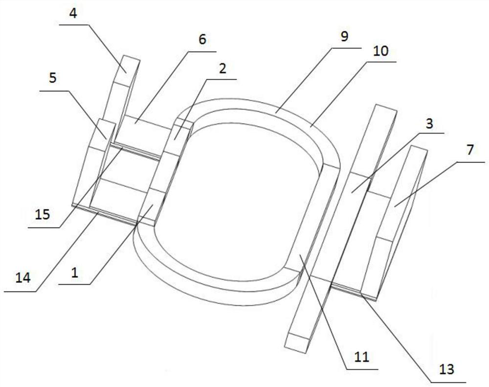
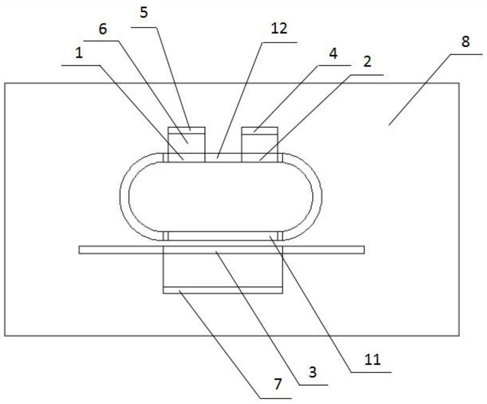
[0039] like figure 1 As shown, a microring coupling modulation structure based on graphene fine-tuning coupling efficiency, specifically includes a microring waveguide structure 9, a signal modulation structure 1, a phase modulation structure 2, and a modulation coupling structure 3, and the entire microring coupling modulation structure is fixed on the substrate 8 on.

[0040] The microring waveguide structure 9 includes two 1 / 2 arc waveguides 10, the upper straight waveguide 12 and the lower straight waveguide 11, the microring waveguide structure 9 is a racetrack structure, and the upper straight waveguide 12 area integrates the signal modulation structure 1 With the phase modulation structure 2, a certain distance is fixed between the lower part of the straight waveguide 11 and the modulation coupling structure 3.

[0041] Graphene is a honeycomb-shaped two-dimensional hexagonal carbon structure material. It is a new type of material. Under the action of an applied voltage,...

Embodiment 2

[0056] Add a bias voltage to the graphene 15 in the phase modulation structure 2, pre-adjust the chemical potential to 0.8eV, and determine the working wavelength of this modulation structure to be 1.548 μm, such as Figure 4 As shown, after the working wavelength is determined, the bias voltage of the graphene 13 in the modulation coupling structure 3 is further adjusted to achieve high-precision regulation of the coupling efficiency.

[0057] Figure 5 It is the relationship between the coupling efficiency and the coupling length of the modulation coupling structure 3 when the working wavelength is 1.548 μm and the coupling spacing is 300 nm. It can be seen from the figure that when the coupling length is 10 μm, the coupling efficiency is 0.9422, which is close to the target value (0.928) .

[0058] Figure 6 When the working wavelength is 1.548 μm and the coupling spacing is 300 nm, the coupling length is determined to be 10 μm, the relationship between the coupling effic...

Embodiment 3

[0060] Add a bias voltage to the graphene 15 in the phase modulation structure 2, pre-adjust the chemical potential to 0.8eV, and then adjust the graphene chemical potential to 0.5eV, and determine the working wavelength of this modulation structure to be 1.5455μm, such as Figure 4 As shown, after the working wavelength is determined, the bias voltage of the graphene 13 in the modulation coupling structure 3 is further adjusted to achieve high-precision regulation of the coupling efficiency.

[0061] Figure 7 is the relationship between the coupling efficiency and the coupling length of the modulation coupling structure 3 when the working wavelength is 1.5455 μm and the coupling spacing is 300 nm. It can be seen from the figure that when the coupling length is 10 μm, the coupling efficiency is 0.9368, which is close to the target value (0.928 ).

[0062] Figure 8 When the working wavelength is 1.5455 μm and the coupling spacing is 300 nm, the coupling length is determined...


PUM

PropertyMeasurementUnit
Radiusaaaaaaaaaa
Lengthaaaaaaaaaa
Lengthaaaaaaaaaa

Abstract

The invention discloses a micro-ring coupling modulation structure based on graphene fine tuning coupling efficiency and an application method thereof; the micro-ring coupling modulation structure comprises a micro-ring waveguide structure, a signal modulation structure, a phase modulation structure and a modulation coupling structure; the micro-ring waveguide structure is a runway type structureand comprises two arc waveguides and two straight waveguides; a signal modulation structure and a phase modulation structure are integrated in the upper straight waveguide area, a certain distance isfixed between the lower straight waveguide area and the modulation coupling structure, and graphene layers are embedded in the signal modulation structure, the phase modulation structure and the modulation coupling structure respectively. According to the micro-ring modulator based on the structure, the coupling efficiency between the micro-ring and the straight waveguide can be finely adjusted, so that the coupling efficiency can reach a desired specific value, the precision is relatively high, the micro-ring modulator plays a role in an application scene in which the coupling efficiency needs to be accurately controlled, and the working wavelength of the structure is tunable; the structure has important application value for a linearized integrated photonic device.

Description

technical field [0001] The invention relates to the field of optoelectronic technology, in particular to a microring coupling modulation structure based on graphene fine-tuning coupling efficiency and a method for using the same. Background technique [0002] As a device that realizes the conversion between electrical signals and optical signals, electro-optical modulators play a vital role in optical communication systems. With the increase in demand for analog modulation, people use various methods to improve the linearity of modulators. For example, circuit pre-compensation technology, feed-forward compensation technology, dual polarization technology, cascade technology and direct coupling scheme and other technologies, but these technologies all contain complex circuits or complex optical paths, making it difficult to compress the cost of devices. [0003] The ultra-linear microring resonator can realize the linear compensation of the optical path to the Mach-Zehnder (M...

Claims


Application Information

Patent Timeline
IPC IPC(8): G02F1/00G02F1/01
CPCG02F1/0018G02F1/011
Inventor 陆荣国沈黎明林瑞吕江泊谭孟王广彪张尚剑李和平刘永
Owner UNIV OF ELECTRONIC SCI & TECH OF CHINA
Why Eureka
Try Eureka