
Low-frequency ultra-wideband wave absorber based on magnetic material and lumped device

An absorbing body and low frequency technology, applied in the field of low frequency ultra-broadband absorbing body, can solve the problems of large size, narrow bandwidth, and unsatisfactory absorbing effect, and achieve the effect of reducing the absorbing frequency band, broadening the bandwidth, and having a simple structure.

Active Publication Date: 2021-01-01
AIR FORCE UNIV PLA
View PDF11 Cites 0 Cited by
  • Summary
  • Abstract
  • Description
  • Claims
  • Application Information

AI Technical Summary

Problems solved by technology

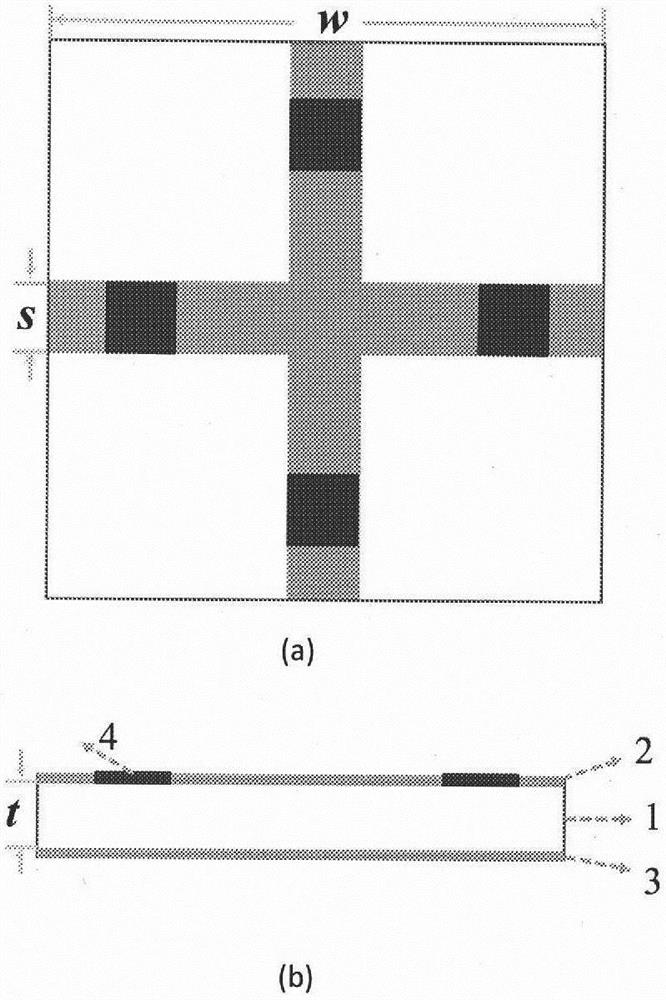
[0003] In order to solve the problems of large size, narrow bandwidth and unsatisfactory absorbing effect when the traditional absorber works in the P-band, the present invention proposes a structural unit, which is hereinafter referred to as "unit", which is characterized in that the unit is a square structure. From top to bottom, it includes a cross-shaped metal patch 2, a dielectric substrate 1, a metal floor 3, and also includes a lumped resistor 4 on the same layer as the cross-shaped metal patch 2;

Method used


Image

  • Low-frequency ultra-wideband wave absorber based on magnetic material and lumped device
  • Low-frequency ultra-wideband wave absorber based on magnetic material and lumped device
  • Low-frequency ultra-wideband wave absorber based on magnetic material and lumped device

Examples


Embodiment Construction

[0026] The low-frequency ultra-broadband absorber based on magnetic materials proposed by the present invention will be specifically described below by describing an embodiment in detail. An example of the embodiment is shown in the accompanying drawings, wherein the same symbols throughout represent the same meanings.

[0027] The formula for calculating the absorption rate of the absorber is: A=1-R, where R represents the reflectivity of the absorber. The embodiments described below by referring to the figures are exemplary only for explaining the present invention and should not be construed as limiting the present invention.

[0028] The present invention is described below in conjunction with accompanying drawing.

[0029] The structural unit of the present invention (hereinafter referred to as "unit") such as figure 1 shown. The unit is a square structure, including a cross-shaped metal patch 2, a dielectric substrate 1, a metal floor 3 from top to bottom, and a lumped...


PUM

PropertyMeasurementUnit
thicknessaaaaaaaaaa
thicknessaaaaaaaaaa
electrical resistanceaaaaaaaaaa

Abstract

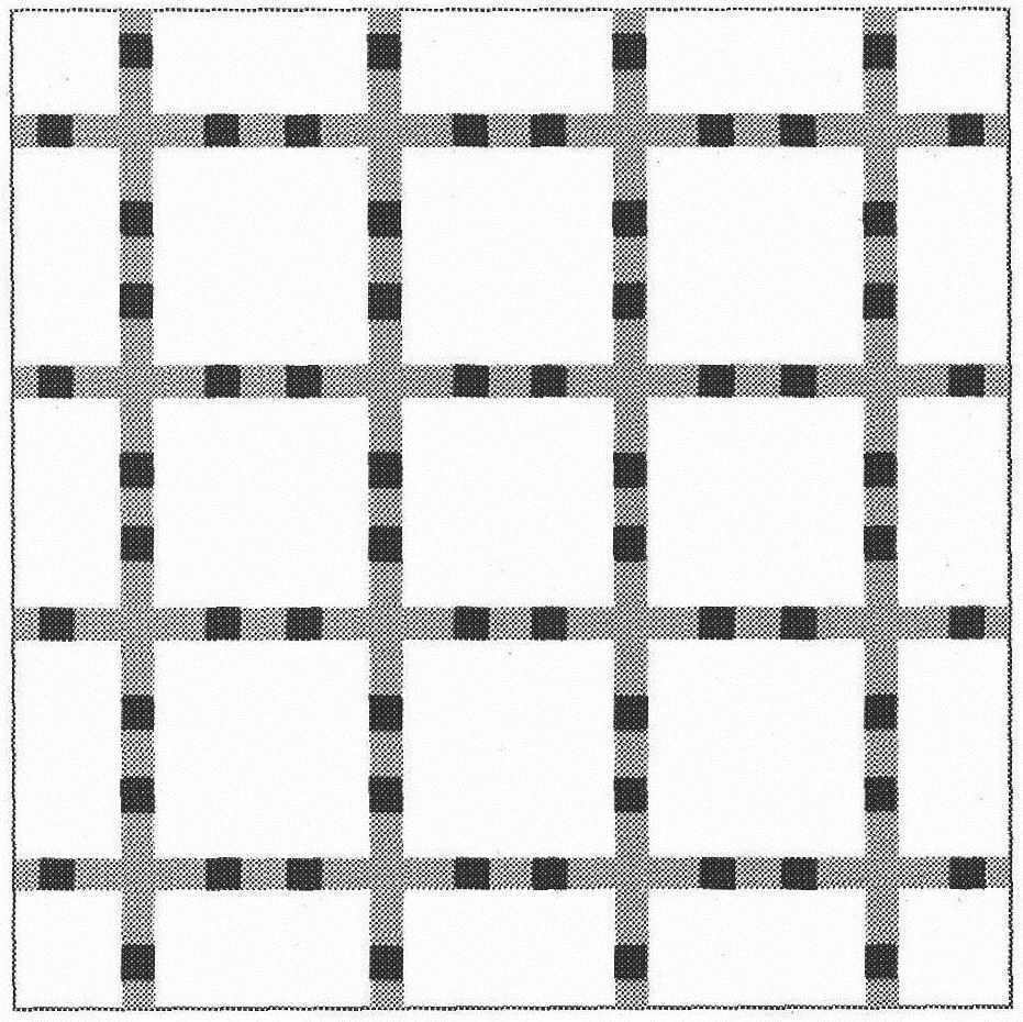
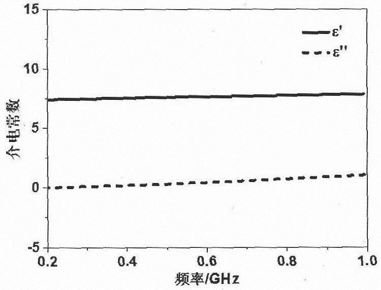
The present invention provides a structure unit, which is of a square structure and comprises a cross-shaped metal patch (2), a dielectric substrate (1), a metal floor (3) and a lumped resistor (4) onthe same layer as the cross-shaped metal patch (2) from top to bottom. The dielectric substrate (1) is a square sheet; the cross-shaped metal patch (2) is attached to the upper surface of the dielectric substrate (1), and two gaps are etched in each of the horizontal branch knot and the vertical branch knot; a lumped resistor (4) is loaded on the gap; and the metal floor (3) completely covers thebottom surface of the dielectric substrate (1). The invention further provides a low-frequency ultra-wideband wave absorber based on the magnetic material and the lumped device, the low-frequency ultra-wideband wave absorber is composed of the structural units and is a linear array or an area array, the larger the number of the structural units in the array is, the better the wave absorbing effect is, and the wave absorbing effect of the area array is remarkably superior to that of the linear array. More than 85% of wave absorbing effect within the frequency band of 0.23 GHz-1. 0GHz is achieved through adoption of a method of combining the magnetic material and the lumped resistor, the problems of narrow P-band wave absorbing bandwidth and unsatisfactory wave absorbing effect are solved,and the ultra-thin P-band wave absorbing material has the advantages of being simple in structure, ultra-thin and miniaturized.

Description

technical field [0001] The invention relates to a broadband absorber, in particular to a low-frequency ultra-broadband absorber based on magnetic materials and lumped devices. Background technique [0002] Metamaterial absorber is a structural artificial electromagnetic material, which utilizes the ohmic loss and dielectric loss of the unit structure to achieve strong absorption of electromagnetic waves, and can reach nearly 100% absorption rate, which has broad application prospects in the field of stealth. But its limitation is that the absorption bandwidth is narrow, and it is difficult to achieve low frequency operation. With the development of advanced low-frequency radar, the absorber needs to have good absorbing performance in the P-band, and most of the existing absorbers work in the L-X band, and there are few researches on the absorber for the P-band . Although the operating frequency of the absorber can be appropriately reduced by increasing the size and thickne...

Claims


Application Information

Patent Timeline
Patent Type & Authority Applications(China)
IPC IPC(8): H01Q17/00
CPCH01Q17/00H01Q17/004H01Q17/008Y02D30/70
Inventor 李桐曹祥玉杨欢欢李思佳吉地辽日田江浩
Owner AIR FORCE UNIV PLA
Learn More