

Structure for optimizing writing performance of magnetic random access memory and preparation method thereof
A technology of random access memory and write performance, applied in static memory, digital memory information, manufacturing/processing of electromagnetic devices, etc., can solve problems such as limited write speed, difficulty in meeting cache, weak, etc., to reduce power consumption, improve Read and write speed, the effect of optimizing write performance
- Summary
- Abstract
- Description
- Claims
- Application Information
AI Technical Summary
Problems solved by technology
Method used
Image

Examples
Embodiment Construction
[0036] In order to make the purpose, technical solutions and advantages of the embodiments of the present invention clearer, the technical solutions in the embodiments of the present invention will be clearly and completely described below in conjunction with the drawings in the embodiments of the present invention. Obviously, the described embodiments It is a part of embodiments of the present invention, but not all embodiments. Based on the embodiments of the present invention, all other embodiments obtained by persons of ordinary skill in the art without making creative efforts belong to the protection scope of the present invention.
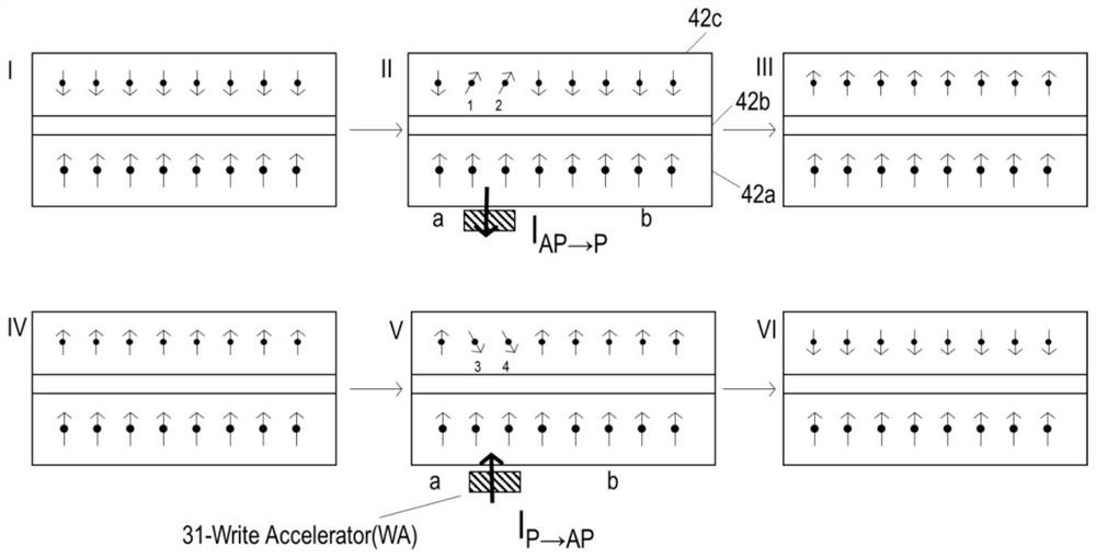
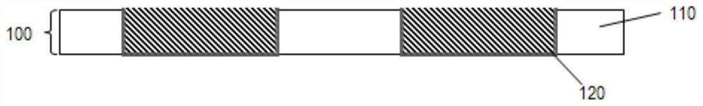
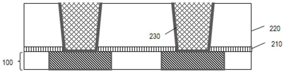
[0037] A structure for optimizing the write performance of a magnetic random access memory (MRAM), comprising: a write accelerator (WriteAccelerator, WA), and the write accelerator (WA) is located on the lower side of the bottom electrode (Bottom Electrode, BE) of the magnetic random access memory (MRAM), The upper side of the bottom electrode ...
PUM
| Property | Measurement | Unit |
|---|---|---|
| Etching depth | aaaaa | aaaaa |
Abstract
Description
Claims
Application Information