Semiconductor structure and forming method thereof

A technology of semiconductors and structural materials, applied in the fields of semiconductor/solid-state device manufacturing, electrical components, circuits, etc., can solve the problems that semiconductor chips cannot achieve the etching effect, cannot meet the integration density of semiconductor chips, and reduce the yield of semiconductor devices. The effect of good etching effect, less defects and high yield

Pending Publication Date: 2021-01-12
SEMICON MFG INT (SHANGHAI) CORP +1
View PDF0 Cites 0 Cited by
  • Summary
  • Abstract
  • Description
  • Claims
  • Application Information

AI Technical Summary

Problems solved by technology

[0003] However, the graphics accuracy of the current self-aligned multiple imaging technology is still not high enough, resulting in the inability to achieve a good etching effect in the process of manufacturing semiconductor chips, thus failing to meet the demand for higher integration density of semiconductor chips, and also reducing Yield of Manufacturing Semiconductor Devices

Method used


Image

  • Semiconductor structure and forming method thereof
  • Semiconductor structure and forming method thereof
  • Semiconductor structure and forming method thereof

Examples


Embodiment Construction

[0034] As mentioned in the background, there is a need to improve the pattern accuracy of current self-aligned multiple imaging techniques.

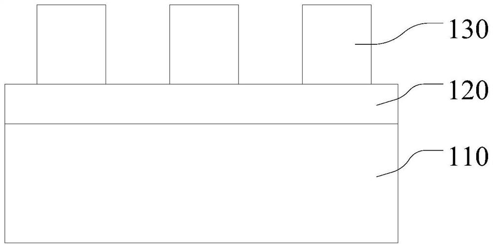
[0035] Figure 1 to Figure 5 It is a schematic diagram of the cross-sectional structure of the pattern formation process of a self-aligned multiple pattern technology.

[0036] Please refer to figure 1 A liner layer 120 is provided on the layer to be etched 110, a sacrificial material layer (not shown) is formed on the surface of the liner layer 120, and the sacrificial material layer is etched to form several discrete sacrificial layers 130;

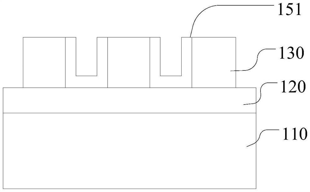
[0037] Please refer to figure 2 , depositing a mask material layer (not shown) on the surface of the liner layer 120 and the surface of the sacrificial layer 130, etching the mask material layer to form a mask structure 151, here figure 2 Two mask structures 151 are schematically drawn;

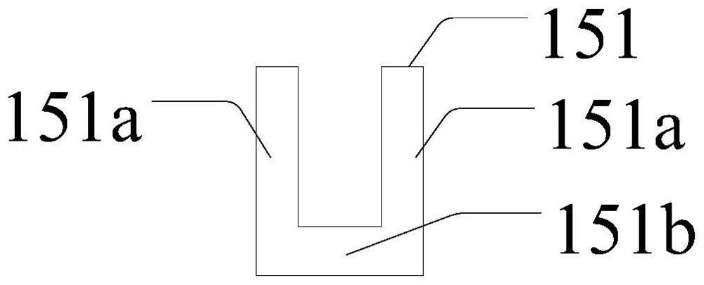
[0038] Please refer to image 3 , the mask structure 151 includes a first portion 151a and a second por...


PUM


Abstract

The invention discloses a semiconductor structure and a forming method thereof, and the forming method comprises the steps: providing a to-be-etched layer, and enabling the surface of the to-be-etchedlayer to be provided with a liner layer; forming a plurality of mutually separated first mask structures on the surface of the liner layer; taking the first mask structure as a mask, etching the to-be-etched layer and the liner layer, forming a groove in the to-be-etched layer, and enabling the first mask structure to form a first initial to-be-removed layer; performing a modification treatment process on the first initial to-be-removed layer to form a first to-be-removed layer; and etching to remove the liner layer and the first to-be-removed layer. The semiconductor structure formed by themethod is good in performance.

Description

technical field [0001] The invention relates to the technical field of semiconductors, in particular to a semiconductor structure and a forming method thereof. Background technique [0002] With the advancement of semiconductor manufacturing technology, in order to achieve faster computing speed, larger data storage capacity and more functions of semiconductor devices, many different methods are used in the prior art to reduce the feature size (CD), reaching The purpose of increasing the integration density of semiconductor chips. Currently, Self-Aligned-Double-Patterning (SADP) and Self-Aligned-Quadra Patterning (SAQP) are gradually being accepted and applied as a solution. [0003] However, the graphics accuracy of the current self-aligned multiple imaging technology is still not high enough, resulting in the inability to achieve a good etching effect in the process of manufacturing semiconductor chips, thus failing to meet the demand for higher integration density of sem...

Claims


Application Information

Patent Timeline
Patent Type & Authority Applications(China)
IPC IPC(8): H01L21/308H01L21/311
CPCH01L21/3086H01L21/31111
Inventor 毕晓峰纪世良张海洋
Owner SEMICON MFG INT (SHANGHAI) CORP
Why Eureka
Try Eureka