LD chip eutectic soldering station

A eutectic welding and chip technology, applied in the field of optical communication, can solve the problems of slow eutectic cooling speed, low substrate positioning accuracy, and low eutectic efficiency

Pending Publication Date: 2021-01-12
广东海信宽带科技有限公司
View PDF0 Cites 1 Cited by
  • Summary
  • Abstract
  • Description
  • Claims
  • Application Information

AI Technical Summary

Problems solved by technology

[0005] The embodiment of the present application provides an LD chip eutectic soldering station to solve the problems of slow eutectic co

Method used


Image

  • LD chip eutectic soldering station
  • LD chip eutectic soldering station
  • LD chip eutectic soldering station

Examples


Embodiment Construction

[0031] The following will clearly and completely describe the technical solutions in the embodiments of the application with reference to the drawings in the embodiments of the application. Apparently, the described embodiments are only some of the embodiments of the application, not all of them. Based on the embodiments in this application, all other embodiments obtained by persons of ordinary skill in the art without creative efforts fall within the protection scope of this application.

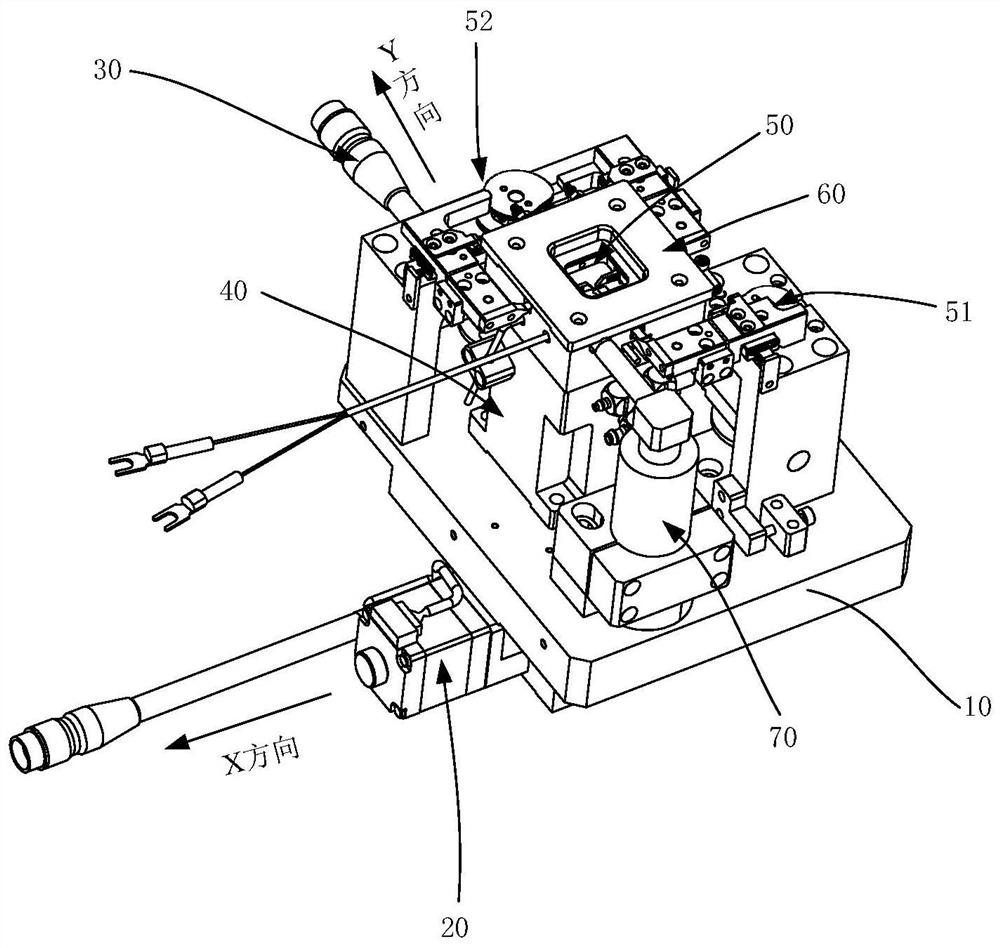
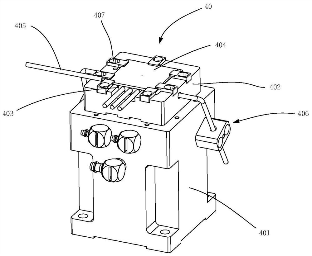
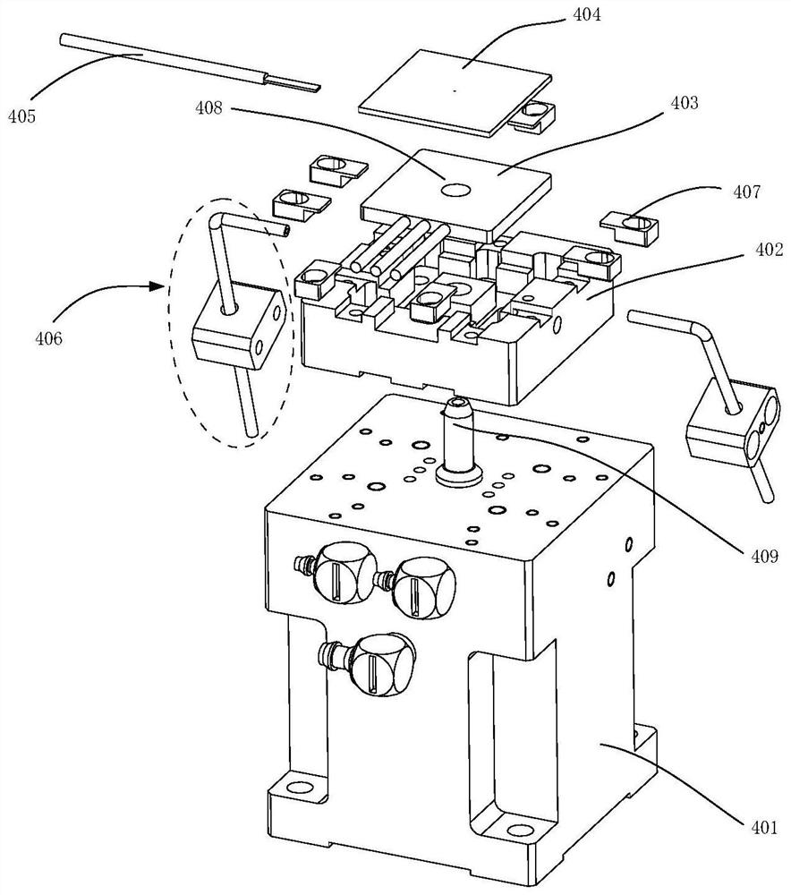
[0032] One of the core links of optical fiber communication is the mutual conversion of optical and electrical signals. Optical fiber communication uses optical signals carrying information to be transmitted in information transmission equipment such as optical fibers / optical waveguides, and the passive transmission characteristics of light in optical fibers / optical waveguides can be used to achieve low-cost, low-loss information transmission; and information processing equipment such as com...


PUM


Abstract

The LD chip eutectic welding table comprises a bottom plate, a substrate positioning mechanism, an XY compensation device, an eutectic temperature control device, a vacuum suction device and an uppereutectic cover, wherein the substrate positioning mechanism, the XY compensation device, the eutectic temperature control device, the vacuum suction device and the upper eutectic cover are fixed to the bottom plate. The eutectic temperature control device comprises a chip stand column, a chip heat insulation block, a ceramic heating piece, an eutectic plate and a cooling blowing system. The vacuumsuction device is used for sucking the substrate onto the eutectic plate; the eutectic upper cover is connected with the chip heat insulation block to form an eutectic cavity, and a through hole communicated with the eutectic cavity is formed in the eutectic upper cover; the substrate positioning mechanism is arranged on the periphery of the eutectic temperature control device and used for positioning a substrate on the eutectic plate in the X direction and the Y direction. The XY compensation device is used for carrying out position compensation on the bottom plate in the X and Y directions;and the cooling blowing system is communicated with the eutectic cavity and is used for cooling the eutectic plate. Through the eutectic temperature control device, the substrate positioning mechanism and the XY compensation device, the LD eutectic efficiency and quality are improved.

Description

technical field [0001] The present application relates to the technical field of optical communication, in particular to an LD chip eutectic soldering station. Background technique [0002] LD (Laser Diode, laser diode), also known as semiconductor laser, is a kind of laser with semiconductor as the working material. In addition to the common characteristics of lasers, it also has small size, light weight, low driving power and current, and high efficiency. , long working life, good beam quality, full curing, direct electrical modulation, etc. Due to these characteristics, the application of semiconductor lasers covers almost the entire field of optoelectronics, and the application in optical fiber communication systems has greatly promoted the development of optical communication technology. [0003] At present, semiconductor lasers are the fastest-growing and most important important light sources for laser optical fiber communications in the field of optical communicatio...

Claims


Application Information

Patent Timeline
IPC IPC(8): H01L21/67H01L21/68H01L21/683H01S5/02
CPCH01L21/67092H01L21/67103H01L21/67109H01L21/68H01L21/6838H01S5/0216
Inventor 冉峥嵘张立赵志颖许伟雄
Owner 广东海信宽带科技有限公司
Why Eureka
Try Eureka