
USB conversion interface device

A technology of USB interface and conversion interface, which is applied in the field of FPGA application, can solve the problems of user design complexity increase, high cost, and inability to communicate in the chip, and achieve the effect of improving design flexibility, reducing complexity, and reducing cost

Pending Publication Date: 2021-01-22
GOWIN SEMICON CORP LTD
View PDF6 Cites 1 Cited by
  • Summary
  • Abstract
  • Description
  • Claims
  • Application Information

AI Technical Summary

Problems solved by technology

[0004] In the system-on-chip architecture based on MCU and FPGA, different interfaces and protocols are used to connect corresponding interface devices. However, because different communication protocols are applied between different interface devices, they cannot communicate with each other on-chip. Set up a dedicated control chip for communication, resulting in increased design complexity and higher cost for users

Method used


Image

  • USB conversion interface device
  • USB conversion interface device
  • USB conversion interface device

Examples


Embodiment Construction

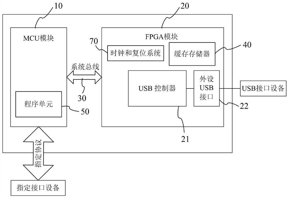
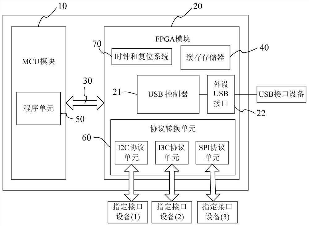
[0029] The traditional system-on-chip architecture based on MCU and FPGA directly uses discrete devices of FPGA and CPU to work, and it is becoming more and more difficult to meet the increasingly large and diverse data processing requirements in terms of performance. However, as described in the background, in the existing system-on-chip architecture based on MCU and FPGA, different interface devices cannot communicate with each other on-chip due to the application of different communication protocols. As a result, the user design complexity is increased, and the cost is also high.

[0030] In order to solve the above problems, the present invention provides a USB conversion interface device, the USB conversion interface device includes an MCU module and an FPGA module interacting through a system bus, wherein the USB conversion interface device utilizes the MCU module and the FPGA module The software and hardware resources of the module perform protocol conversion to realize...


PUM


Abstract

The invention relates to a USB conversion interface device. The USB conversion interface device comprises an MCU (Microprogrammed Control Unit) module and an FPGA (Field Programmable Gate Array) module which are interacted through a system bus, wherein the USB conversion interface device performs protocol conversion by utilizing software and hardware resources of the MCU module and the FPGA moduleto realize interconnection between USB interface equipment and specified interface equipment; a problem that the USB interface equipment cannot be directly communicated with interface equipment adopting other communication protocols can be solved. According to the USB conversion interface device, the application scene of the system-on-chip based on the MCU and the FPGA is broadened, the design flexibility is improved, design complexity of a user is reduced, and cost is reduced.

Description

technical field [0001] The invention relates to the field of FPGA applications, in particular to a USB conversion interface device. Background technique [0002] In the Internet of Things solution, the microcontroller (Micro-controllerUnit, hereinafter referred to as MCU) plays the role of the core "core". However, with the improvement and iteration of the intelligence of the Internet of Things, in order to meet the requirements of performance, scalability and integration, the microcontroller is also developing from a single chip to a more highly integrated device, namely "MCU+". [0003] Utilizing the programmable features of Field Programmable Gate Array (FPGA), and introducing the System on Chip (SoC) architecture implemented by FPGA and microcontroller, it can freely expand external devices according to different application scenarios , has good scalability, meets the needs of different application fields, and can be used in products or system platforms such as various ...

Claims


Application Information

Patent Timeline
IPC IPC(8): G06F13/42
CPCG06F13/4282G06F2213/0042G06F2213/0016G06F2213/3852Y02D10/00
Inventor 杜金凤刘春香刘锴任程程张茹
Owner GOWIN SEMICON CORP LTD
Features
  • Generate Ideas
  • Intellectual Property
  • Life Sciences
  • Materials
  • Tech Scout
  • Unparalleled Data Quality
  • Higher Quality Content
  • 60% Fewer Hallucinations
Learn More