Display panel, preparation method thereof and display device

A display panel and backplane technology, which is applied in semiconductor/solid-state device manufacturing, electrical components, electric solid-state devices, etc., can solve the problems of large surface resistance, obvious voltage drop, uneven brightness, etc. The effect of reduction and uniform brightness

Active Publication Date: 2021-01-22
HEFEI BOE ZHUOYIN TECH CO LTD +1
View PDF6 Cites 0 Cited by
  • Summary
  • Abstract
  • Description
  • Claims
  • Application Information

AI Technical Summary

Problems solved by technology

[0003] Top-emitting OLED devices mainly include a transparent cathode, an organic functional layer and a reflective anode. The light emitted by the organic functional layer must pass through the transparent cathode, so the transparent cathode needs to be made very thin to achieve high transmittance. However, after the transparent cathode is thinned, The surface resistance is very large, and the voltage drop is particularly obvious, resulting in uneven brightness during display

Method used


Image

  • Display panel, preparation method thereof and display device
  • Display panel, preparation method thereof and display device
  • Display panel, preparation method thereof and display device

Examples


Embodiment Construction

[0061] Example embodiments will now be described more fully with reference to the accompanying drawings. Example embodiments may, however, be embodied in many forms and should not be construed as limited to the embodiments set forth herein; rather, these embodiments are provided so that this disclosure will be thorough and complete, and will fully convey the concept of example embodiments to those skilled in the art. The same reference numerals in the drawings denote the same or similar structures, and thus their detailed descriptions will be omitted.

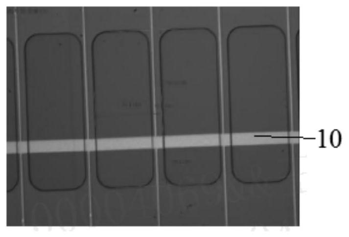
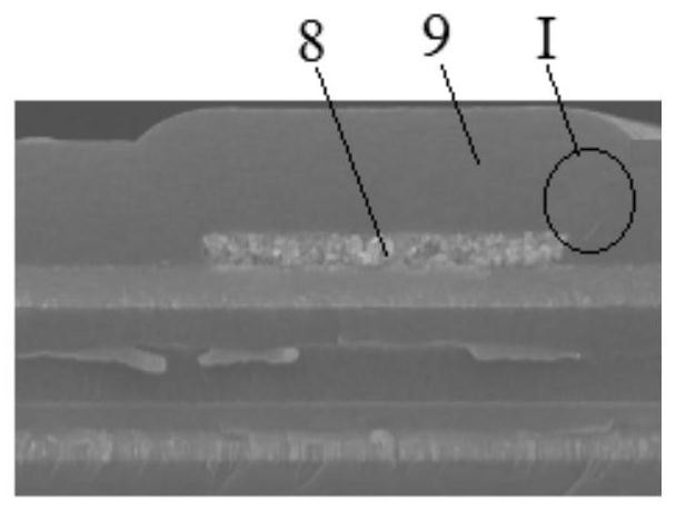
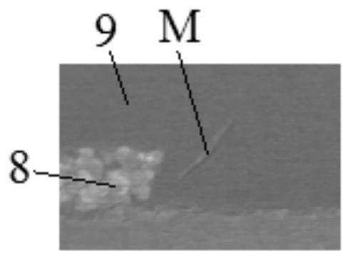
[0062] At present, in related technologies, the auxiliary electrode 8 can be directly printed on the OLED device. However, the limit line width printed by the existing nozzle is about 20um, and the auxiliary electrode 8 will cover the light-emitting area, resulting in a decrease in aperture ratio and brightness. . There are also some related technologies that use the transfer printing process, but the maximum single printing ...


PUM

PropertyMeasurementUnit
heightaaaaaaaaaa
thicknessaaaaaaaaaa

Abstract

The invention relates to the technical field of display, and provides a display panel, a preparation method thereof, and a display device. The display panel comprises a backplane, a first electrode, an auxiliary layer, a pixel defining layer, a light-emitting layer group, a second electrode and an auxiliary electrode; the first electrode is arranged on one side of the backplane, and the face, awayfrom the backplane, of the first electrode is a first plane; the auxiliary layer is arranged on the same side of the backplane as the first electrode, the side, away from the backplane, of the auxiliary layer is a second plane, and the second plane and the first plane are coplanar or the second plane is farther away from the backplane than the first plane; the pixel defining layer is arranged onone side, far away from the backplane, of the auxiliary layer; the light-emitting layer group is assembled on one side, far away from the backplane of the first electrode; the second electrode is arranged on one side, far away from the backplane, of the light-emitting layer group; the auxiliary electrode is arranged on the side, away from the backplane, of the second electrode, and the orthographic projection of the auxiliary electrode on the backplane is located in the orthographic projection of the pixel defining layer on the backplane. The pixel defining layer of the display panel does notgenerate wrinkles and is uniform in brightness.

Description

technical field [0001] The present invention relates to the field of display technology, in particular to a display panel, a method for preparing the display panel, and a display device including the display panel. Background technique [0002] Compared with LCD (Liquid Crystal Display, liquid crystal) display, OLED (Organic Electroluminescence Display, organic light-emitting semiconductor) display has the characteristics of self-luminescence, high luminous efficiency, low operating voltage, light and thin, flexible and simple manufacturing process, etc. Wide range of applications. OLED display can be divided into top-emitting and bottom-emitting according to the light-emitting surface. Because top-emitting OLED has a high aperture ratio, it has been widely concerned and researched. [0003] Top-emitting OLED devices mainly include a transparent cathode, an organic functional layer and a reflective anode. The light emitted by the organic functional layer must pass through t...

Claims


Application Information

Patent Timeline
Patent Type & Authority Applications(China)
IPC IPC(8): H01L27/32H01L51/52H01L51/56
CPCH10K59/122H10K50/824H10K50/828H10K59/1201H10K71/00
Inventor 王欣欣许名宏
Owner HEFEI BOE ZHUOYIN TECH CO LTD
Why Eureka
Try Eureka