Ceramic electronic device

A technology of electronic components and ceramics, applied in the field of ceramic electronic components, can solve the problems of inability to meet thermal shock resistance or high temperature load life, and achieve the effects of good thermal shock resistance, improved installation reliability, and good high temperature load life.

Active Publication Date: 2021-01-29
TDK CORPARATION
View PDF9 Cites 2 Cited by
  • Summary
  • Abstract
  • Description
  • Claims
  • Application Information

AI Technical Summary

Problems solved by technology

[0006] However, in the technique of Patent Document 1, when a more severe thermal load of about 200°C is applied, there is a possibility that the thermal shock resistance and the high-temperature load life cannot be satisfied.

Method used


Image

  • Ceramic electronic device
  • Ceramic electronic device
  • Ceramic electronic device

Examples


Embodiment

[0130] Hereinafter, the present invention will be described based on more detailed examples, but the present invention is not limited to these examples.

[0131] (Experiment 1)

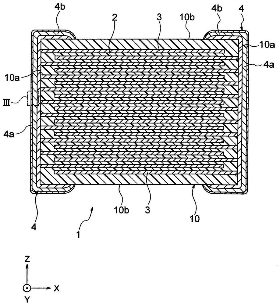
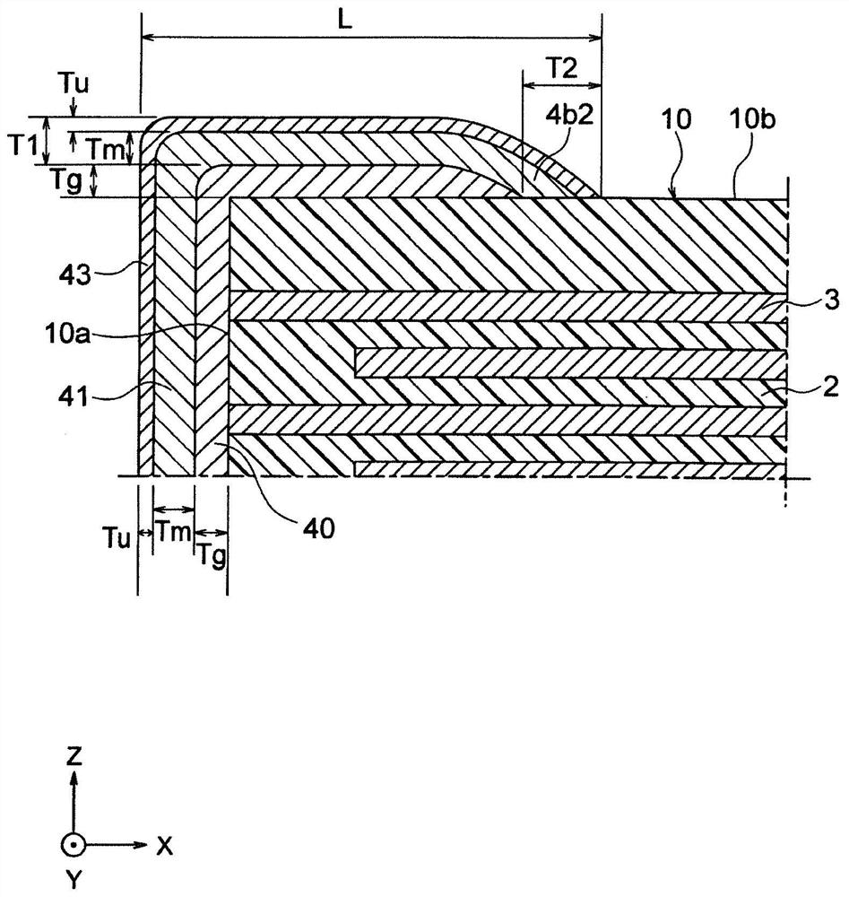
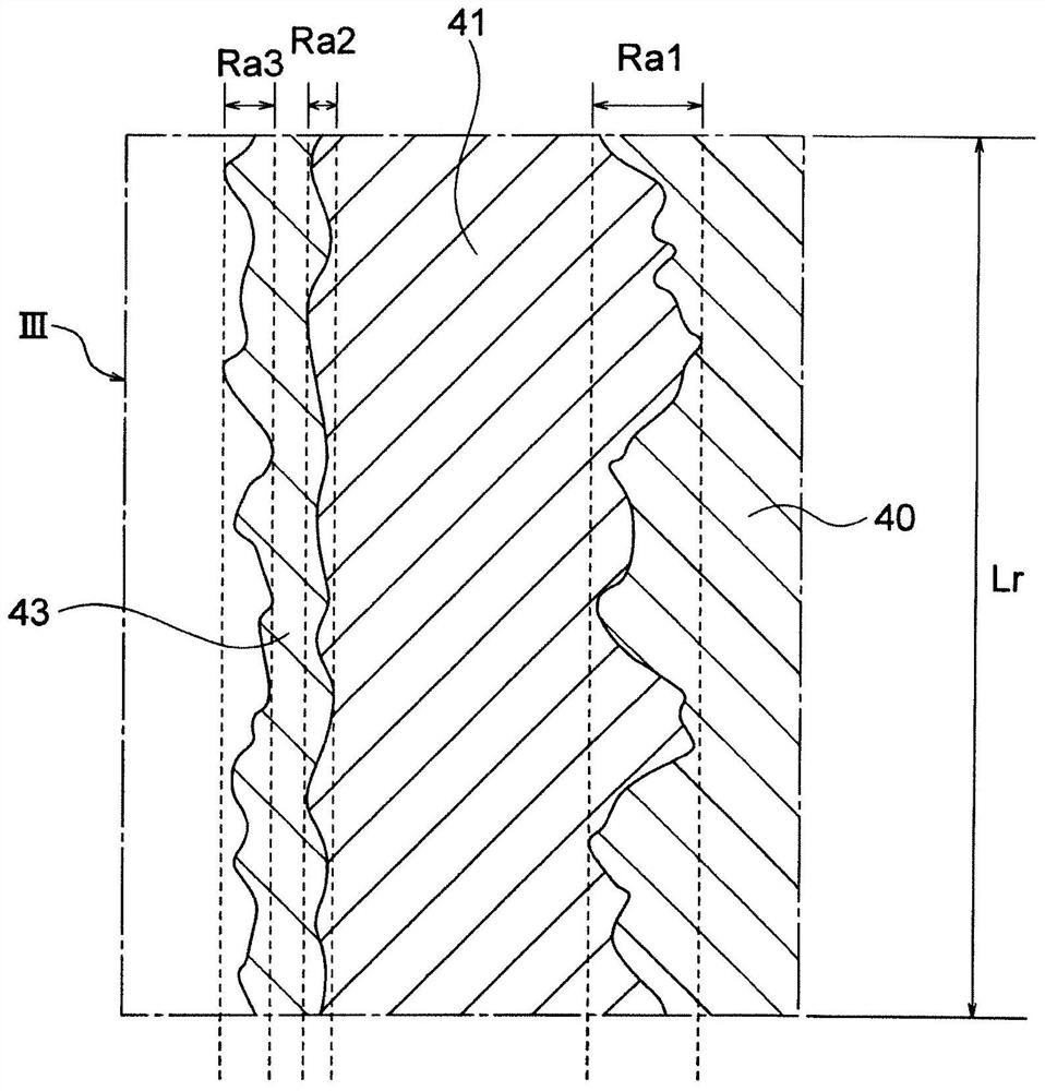
[0132] In Experiment 1, capacitor samples according to Examples 1 to 20 were produced. As the ceramic body 10 of each capacitor sample, CaZrO laminated with CaZrO 3 A sintered body sample of the ceramic layer 2 as the main component and the internal electrode layer 3 containing Ni. Then, with respect to this sintered body sample, a pair of external electrodes 4 were formed in the following procedure.

[0133] First, a metal paste to be a raw material of the base electrode layer 40 is prepared. This metal paste is obtained by preparing and kneading a metal powder, a glass component, and a vehicle at a predetermined ratio. The glass components used at this time use ZnO, B 2 o 3 , SiO 2 、Al 2 o 3 As a raw material, additionally, a mixture selected from BaCO 3 , CaCO 3 , SrCO 3 , MgCO 3 , or ...


PUM

PropertyMeasurementUnit
surface roughnessaaaaaaaaaa
thicknessaaaaaaaaaa
surface roughnessaaaaaaaaaa

Abstract

The present invention relates to a ceramic electronic device including a ceramic body having ceramic layers and internal electrode layers stacked in alternating manner and a terminal electrode formedat an end face of the ceramic body. The terminal electrode includes a base electrode including a metal component and a glass component, an intermediate electrode layer including Ni and formed at an outer face of the base electrode layer, and an upper electrode layer including Pd or Au and formed at an outer face of the intermediate electrode layer. Also, a surface roughness Ra1 of the base electrode layer in the terminal electrode is 5[mu]m or less; or the surface roughness Ra1 of the base electrode layer, a surface roughness Ra2 of the intermediate electrode layer, and a surface roughness Ra3of the upper electrode layer satisfy a relationship of Ra1>Ra3>=Ra2.

Description

technical field [0001] The present invention relates to a ceramic electronic component formed with external electrodes. Background technique [0002] Electronic components such as a plurality of ceramic electronic components are mounted inside the electronic equipment. [0003] Currently, in the mounting of these electronic components, lead-free solders such as Sn-Ag-Cu based solders, conductive adhesives in which conductive fine particles such as metal fillers are added to thermosetting resins such as epoxy resins, etc. are used as bonding materials. . The selection of these bonding materials is mainly determined by the use environment. [0004] In recent years, in inverter circuits and the like using SiC power semiconductors, the operating environment is assumed to exceed 150°C. Therefore, in such a circuit board, a mounting technique capable of maintaining a stable bonding force (that is, high mounting reliability) is required even when a thermal load is applied. To m...

Claims


Application Information

Patent Timeline
Patent Type & Authority Applications(China)
IPC IPC(8): H01G4/232H01G4/30H01G4/12
CPCH01G4/232H01G4/2325H01G4/30H01G4/12
Inventor 高桥哲弘福冈智久
Owner TDK CORPARATION
Why Eureka
Try Eureka