Member for electronic circuit, method for manufacturing the member, and electronic part

a technology for electronic circuits and members, applied in the direction of printed circuit manufacturing, insulating substrate metal adhesion improvement, etc., can solve the problems of increasing the temperature of those semiconductor devices, the ineffectiveness of semiconductor devices to sufficiently radiate heat generated, and the large amount of electric energy consumed by transistors and semiconductor rectifiers per operating area, etc., to achieve the effect of reducing the number of manufacturing steps, reducing the manufacturing cost, and increasing reliability

Inactive Publication Date: 2003-06-05
NGK INSULATORS LTD
View PDF4 Cites 48 Cited by
  • Summary
  • Abstract
  • Description
  • Claims
  • Application Information

AI Technical Summary

Benefits of technology

0090] Therefore, it is not necessary to interpose an Ni plated layer, a solder layer, an Ni layer, and a lower electrode layer between the heat sink 20 and the insulating substrate 24, but only the first joint member 26 may be interposed between the heat sink 20 and the insulating substrate 24. Consequently, the number of manufacturing steps is greatly reduced, and hence the manufacturing cost is effectively lowered.
0091] According to the first embodiment, the coefficient of thermal expansion of the insulating substrate 24, the first joint member 26, and the heat sink 20 is in the range from 3.0.times.10.sup.-6 to 1.0.times.10.sup.-5/K. Therefore, after the IC chip 16 is installed on the member 12A, making up the electronic component 10A, when the temperature of the IC chip 16 is increased due to the usage of the electronic component 10A, the heat sink 20 and the insulating substrate 24 are not peeled off each other. As a result, the electronic component 10A has its reliability increased.
0092] According to the first embodiment, inasmuch as the first joint member 26 is made of a hard brazing material containing an active element, the first joint member 26 has a more excellent heat radiation capability than if it comprises a solder layer. The heat from the IC chip 16 can efficiently be transferred to the heat sink 20, so that the electronic component 10A can easily be designed thermally. Even when the electronic component 10A is subjecte...

Problems solved by technology

Semiconductor devices such as power transistors and semiconductor rectifiers consume a large amount of electric energy per operating area, and cases (packages) and leads of such semiconductor devices may not be effective enough to sufficiently radiate heat generated thereby.
Therefore, the internal temperature of those semiconductor devices tend to increase to such a level that the semiconductor devices may suffer a thermal breakdown.
Semiconductor devices of greater size are liable to peel off position or be mechanically broken due to increased stresses which are caused by the difference between the coefficient of thermal expansion of the semiconductor substrate (including a semiconductor device of silicon or GaAs and an insulating substrate of AlN or Si.sub.3N.sub.4) and the coefficient of thermal expansion of the heat sink.
However, these heat sink materials hardly satisfy market ...

Method used


Image

  • Member for electronic circuit, method for manufacturing the member, and electronic part
  • Member for electronic circuit, method for manufacturing the member, and electronic part
  • Member for electronic circuit, method for manufacturing the member, and electronic part

Examples


Embodiment Construction

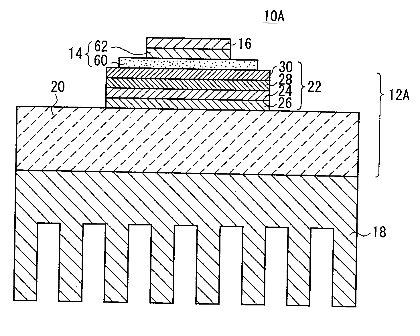
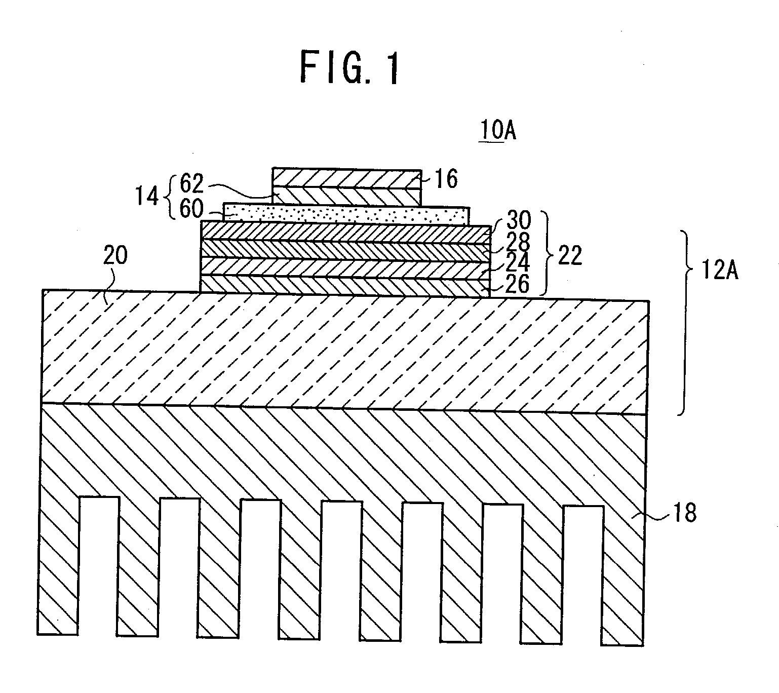
, the insulating substrate 24 was an insulating substrate of AlN (aluminum nitride) having a coefficient of thermal conductivity of 180 W / mK, a size of 40.times.50 mm, and a thickness of 0.635 mm, the electrode 30 was an electrode of Cu (pure copper) having a size of 35.times.45 mm and a thickness of 0.30 mm, and the heat sink 20 was made of a C / Cu composite material having a size of 50.times.80 mm and a thickness of 3.0 mm.

[0100] The first and second joint members 26, 28, each in the form of a sheet of a commercial brazing material of Ag--Cu--Ti (Ag--35.25 Cu--1.75 Ti) having a thickness of 50 .mu.m, were placed respectively between the insulating substrate 24 and the heat sink 20 and between the electrode 30 and the insulating substrate 24. The assembly was then held in a vacuum of 0.00133 Pa at a given temperature (850.degree. C.) for 10 minutes, and then annealed, producing a joined assembly (the member 12A).

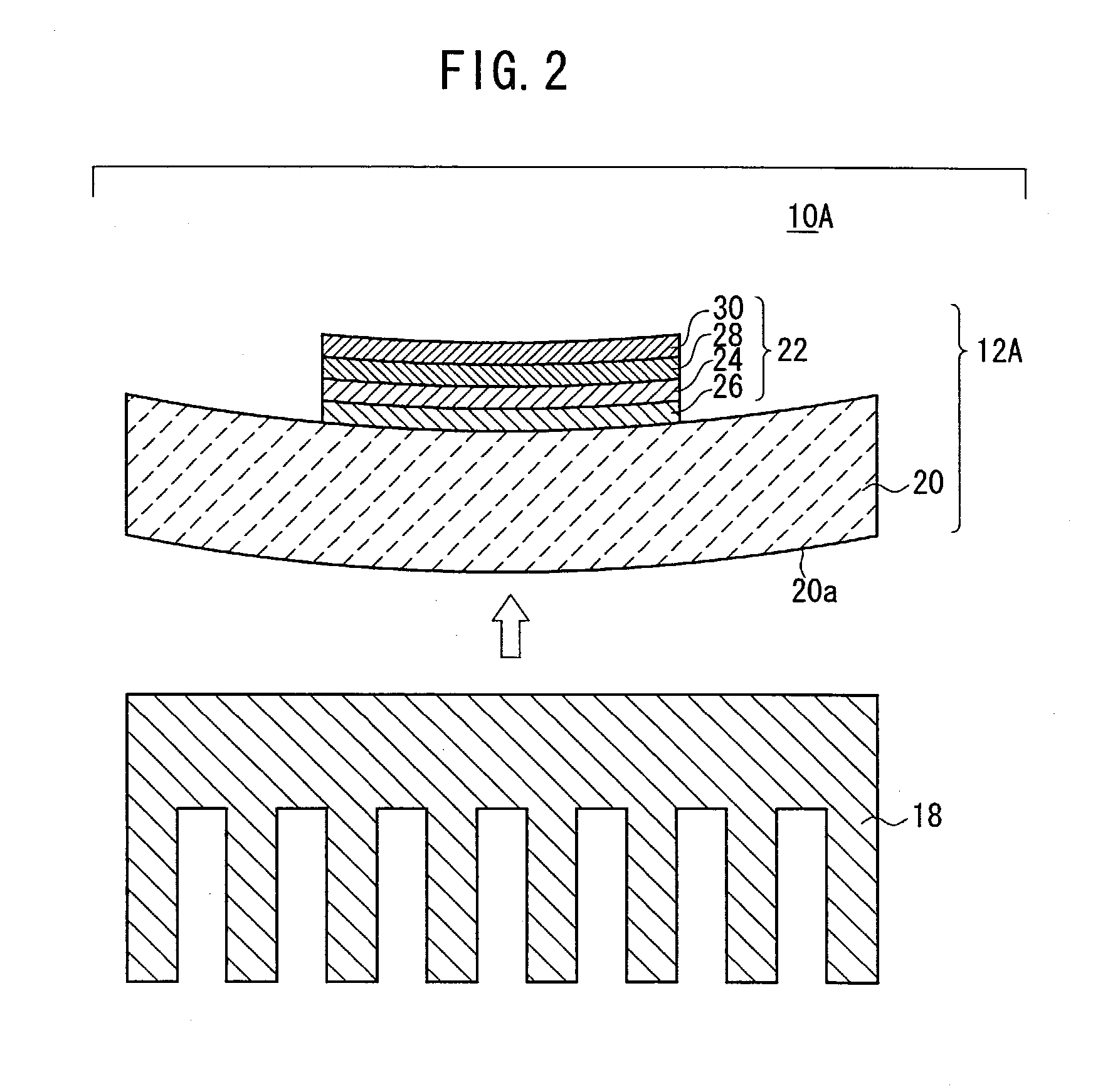
[0101] When the temperature was raised and lowered, the member 12A was ...


PUM


Abstract

A member (12A) for use in an electronic circuit has a thermally conductive layer (22) mounted on a heat sink (20). The thermally conductive layer (22) comprises an insulating substrate (24), a first joint member (26) joining the insulating substrate (24) to the heat sink (20) and containing an active element, a second joint member (28) disposed on the insulating substrate (24), and an electrode (30) disposed on the second joint member (28). The insulating substrate (24) comprises an AlN layer or an Si3N4 layer. Each of the first and second joint members (26, 28) is made of a hard brazing material containing an active element. The heat sink (20) is made of an SiC/Cu composite material or a C/Cu composite material.

Description

[0001] The present invention relates to a member for use in an electronic circuit for cooling an electronic circuit chip composed of semiconductors, etc., a method of manufacturing such a member, and an electronic component.[0002] Generally, semiconductor devices are highly susceptible to heat, and should be designed such that their internal temperature will not exceed an allowable maximum temperature at a junction area of said semiconductor devices. Semiconductor devices such as power transistors and semiconductor rectifiers consume a large amount of electric energy per operating area, and cases (packages) and leads of such semiconductor devices may not be effective enough to sufficiently radiate heat generated thereby. Therefore, the internal temperature of those semiconductor devices tend to increase to such a level that the semiconductor devices may suffer a thermal breakdown.[0003] The above phenomenon also occurs in semiconductor devices incorporating CPUs. As the clock freque...

Claims


Application Information

Patent Timeline
IPC IPC(8): H01L23/373H05K1/03H05K3/00H05K3/38
CPCH01L23/3735H01L2224/325H01L2924/3511H05K1/0306H05K3/0058H01L2924/13055H05K3/38H01L2924/01019H01L2924/00H01L23/373
Inventor ISHIKAWA, SHUHEIISHIKAWA, TAKAHIROKIDA, MASAHIROSUZUKI, KEN
Owner NGK INSULATORS LTD
Why Eureka
Try Eureka