
Detector chip assembly for receiving high-speed optical signals

A detector chip, optical signal technology, applied in semiconductor devices, electrical components, circuits, etc., can solve problems such as inability to apply 50Gbps network, insufficient to ensure 50Gbps signal reception, etc., to ensure mass production and increase effective reception bandwidth. , good reliability

Pending Publication Date: 2021-01-29
欧润光电科技(苏州)有限公司
View PDF0 Cites 2 Cited by
  • Summary
  • Abstract
  • Description
  • Claims
  • Application Information

AI Technical Summary

Problems solved by technology

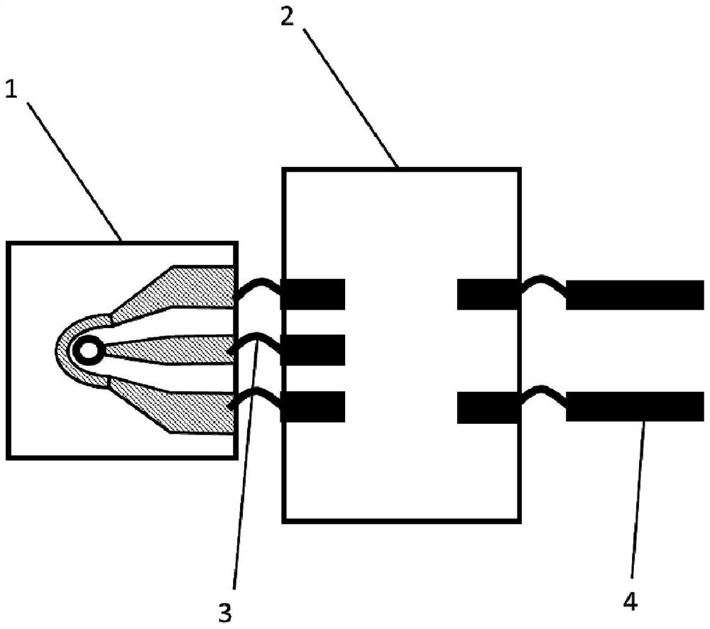
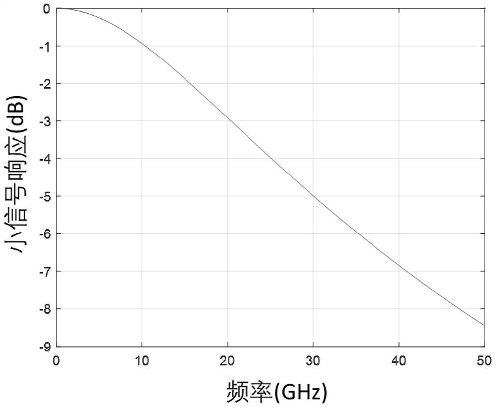
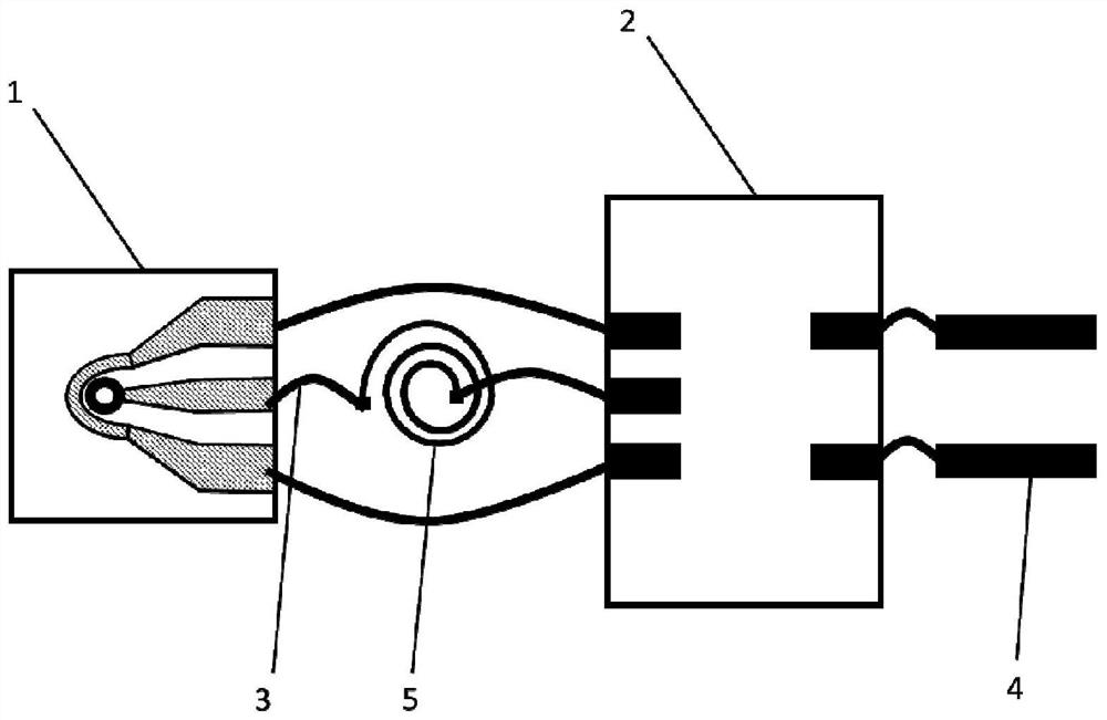
Although the bandwidth of the detector can be increased from 20.4GHz to 29.1GHz by introducing an inductor, but to receive a 50Gbps optical signal, it is generally required that the 3dB bandwidth of the detector should be above 33GHz, so just adding an inductor is still not enough to guarantee a 50Gbps signal reception, cannot be applied to 50Gbps network

Method used


Image

  • Detector chip assembly for receiving high-speed optical signals
  • Detector chip assembly for receiving high-speed optical signals
  • Detector chip assembly for receiving high-speed optical signals

Examples


Embodiment 1

[0051] Such as Figure 5 As shown, the detector chip assembly used for high-speed optical signal reception in the present invention includes a detector chip 1, a TIA2, an inductor 5, a capacitor 6 and leads 4 connected to external circuits, the detector chip 1, TIA2, The inductor 5 and the capacitor 6 are pasted on the same substrate 7; there is a metal film on the substrate 7; the detector chip 1 is connected to one end of the inductor 5 through the first gold wire 3, and the other end of the inductor 5 is connected to one end of the capacitor 6, The end of the capacitor 6 is connected to the TIA2 through the second gold wire; the other end of the capacitor 6 is grounded; the capacitor 6 is connected in parallel with the inductor 5 and the TIA2; the lead 4 can output high-speed electrical signals.

[0052] As a preferred embodiment, the inductance 5 and the capacitor 6 can be made by a thin film process and integrated on the substrate 7 to facilitate packaging and save costs;...

Embodiment 2

[0060] Example 2

[0061] Such as Figure 8 As shown, the inductor 5 originally located on the same substrate 7 as the capacitor 6 is replaced by a first gold wire 3 of a certain length; the first gold wire 3 not only provides the connection between the capacitor 6 and the detector chip 1, but also acts as an inductor 5 role. Compared with Example 1, Example 2 uses gold wires instead of inductor 2, which not only reduces the cost, but also because the length of gold wires can be adjusted during chip packaging, the inductance value also changes accordingly, so gold wires of different lengths will Can play the role of adjustable inductance. Since the parameters of detector chips from different suppliers are different, adjusting the inductance value by changing the length of the first gold wire will greatly facilitate the adjustment of resonance characteristics for different detector chips to obtain the best response performance. The size of the first gold wire 3 is adjusted a...


PUM

PropertyMeasurementUnit
lengthaaaaaaaaaa
capacitanceaaaaaaaaaa
lengthaaaaaaaaaa

Abstract

The invention discloses a detector chip assembly for receiving high-speed optical signals. The detector chip assembly comprises a detector chip, at least two sections of gold wires, a TIA, at least two lead wires which are connected with an output end of the TIA and are used for realizing connection with an external circuit, a capacitor positioned between the detector chip and the TIA; wherein oneend of the capacitor and the detector chip shares a common ground; the capacitor is connected with the TIA in parallel; and the first gold wire is connected with the detector chip and the capacitor,and the second gold wire is connected with the capacitor and the TIA. The detector chip converts a received high-speed modulated optical signal into an electric signal, and the electric signal is input into the TIA through the inductance capacitor, amplified by the TIA and then input into an external circuit through the lead. By selecting proper inductance and capacitance, the effective receivingbandwidth of the detector chip can be greatly increased, so that the high-speed optical signal receiving is realized by utilizing the low-cost and low-bandwidth detector chip.

Description

technical field [0001] The invention relates to a signal transmission device in the communication field, in particular to a detector chip assembly for high-speed optical signal reception. Background technique [0002] With the explosive growth of information brought about by the application of high-definition video, 5G mobile communication and other technologies and the popularization of the Internet of Things, communication networks are facing increasing pressure on bandwidth growth. The traditional 10G transmission technology is no longer enough to meet the current bandwidth requirements, and the development of 100G / 400G / 800G transmission technology has become inevitable. However, there are many challenges in the process of upgrading from the traditional 10G network to 100G and beyond, one of which is the demand for high-bandwidth, low-cost and reliable detector chips for high-speed optical signal reception. [0003] The bandwidth of the semiconductor photodiode detector ...

Claims


Application Information

Patent Timeline
Patent Type & Authority Applications(China)
IPC IPC(8): H01L31/0203H01L31/02
CPCH01L31/02002H01L31/02016H01L31/0203
Inventor 王中和刘小红
Owner 欧润光电科技(苏州)有限公司
Learn More