Flexible circuit board and manufacturing method thereof

A technology of flexible circuit boards and manufacturing methods, which is applied in the fields of printed circuit manufacturing, printed circuits, printed circuits, etc., can solve problems such as unsatisfactory requirements, and achieve the effect of improving visible light transmittance

Active Publication Date: 2021-01-29
深圳市顺华智显技术有限公司
View PDF7 Cites 0 Cited by
  • Summary
  • Abstract
  • Description
  • Claims
  • Application Information

AI Technical Summary

Problems solved by technology

Conventional flat LED displays can no...

Method used


Image

  • Flexible circuit board and manufacturing method thereof

Examples


Embodiment 1

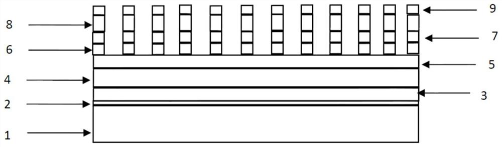
[0093] The flexible circuit board provided in this embodiment includes a flexible base material, and the material of the flexible base material is PET (transparent polyethylene resin), which is sequentially formed on the flexible base material from bottom to top;

[0094] a transition layer 2 with a thickness of 1 nm, made of simple silicon;

[0095] An optical anti-reflection layer 3 with a thickness of 15nm, made of silicon oxide;

[0096] The optical anti-reflection layer 4 with a thickness of 30nm is made of niobium oxide;

[0097] A protective transition layer 5 with a thickness of 5 nm, made of silicon oxide;

[0098] A transition layer 6 with a thickness of 5 nm, made of elemental nickel;

[0099] A seed layer 7 with a thickness of 20nm, made of simple copper;

[0100] Copper layer 8 with a thickness of 10 μm; and

[0101] The protective layer 9 with a thickness of 100 nm is made of simple nickel.

[0102] The preparation method comprises the following steps:

[0...

Embodiment 2

[0115] The flexible circuit board provided in this embodiment includes a flexible substrate, and the material of the flexible substrate is PI (transparent polyimide), which is sequentially formed on the flexible substrate from bottom to top;

[0116] A transition layer 2 with a thickness of 3nm, made of elemental zirconium;

[0117] The optical anti-reflection layer 3 with a thickness of 25nm is made of silicon nitride;

[0118] An optical anti-reflection layer 4 with a thickness of 60nm, made of silicon oxide;

[0119] A protective transition layer 5 with a thickness of 10 nm, made of silicon oxide;

[0120] The transition layer 6 with a thickness of 20nm is made of elemental silver;

[0121] A seed layer 7 with a thickness of 150nm, made of simple copper;

[0122] Copper layer 8 with a thickness of 25 μm; and

[0123] The protective layer 9 with a thickness of 1000nm is made of elemental silver.

[0124] The preparation method comprises the following steps:

[0125] A ...

Embodiment 3

[0137] The flexible circuit board provided in this embodiment includes a flexible substrate, and the material of the flexible substrate is PI (transparent polyimide), which is sequentially formed on the flexible substrate from bottom to top;

[0138] A transition layer 2 with a thickness of 5 nm, made of elemental chromium;

[0139] The optical anti-reflection layer 3 with a thickness of 50nm is made of silicon nitride;

[0140] The optical anti-reflection layer 4 with a thickness of 100nm is made of titanium oxide;

[0141] A protective transition layer 5 with a thickness of 200nm, made of silicon oxide;

[0142] The transition layer 6 with a thickness of 200nm is made of elemental gold;

[0143] A seed layer 7 with a thickness of 300nm, made of simple copper;

[0144] A copper layer 8 with a thickness of 35 μm, made of simple copper; and

[0145] The protective layer 9 with a thickness of 2000nm is made of simple tin.

[0146] The preparation method comprises the follow...


PUM

PropertyMeasurementUnit
Thicknessaaaaaaaaaa
Thicknessaaaaaaaaaa
Thicknessaaaaaaaaaa

Abstract

The invention relates to a flexible circuit board and a manufacturing method thereof. The flexible circuit board comprises a flexible base material 1 which is provided with a transition layer 2, an optical antireflection layer 3, an optical antireflection layer 4, a protective transition layer 5, a transition layer 6, a seed layer 7, a copper layer 8 and a protective layer 9 from bottom top to top. The manufacturing method comprises the steps of (1) plating and (2) etching the circuit. According to the invention, the transition layer, the protective layer and the seed layer are introduced between the flexible substrate 1 and the conductive copper layer 8, so that the adhesive force between the substrate and the conductive copper is improved, the copper foil with the thickness of 20-30 microns can be electroplated on the surface of the substrate, and the drawing force of the bonding pad can reach more than 1N. According to the invention, the optical antireflection layer 3 and the optical antireflection layer 4 are introduced and form an optical anti-reflection structure, so that the visible light transmittance of the circuit board is improved, and the loss value of the transmittancecan be reduced to less than 5%.

Description

technical field [0001] The invention relates to the technical field of circuit boards, in particular to a flexible circuit board and a manufacturing method thereof. Background technique [0002] The LED electronic display screen is composed of hundreds to hundreds of thousands of light-emitting diodes evenly arranged in a matrix, and is used to display various information such as text, graphics, images, animations, videos, and video signals. Conventional flat LED displays can no longer meet the needs of the modern market. Flexible LED displays are attracting more and more attention because they can meet various shapes (for example, they can be cylindrical, inner arc, ribbon, spiral, etc.). Contents of the invention [0003] The first purpose of the present invention is to provide a flexible circuit board. The flexible transparent circuit board can be applied to flexible LED display screens. It has good bonding performance with glass walls of different shapes, and can play...

Claims


Application Information

Patent Timeline
IPC IPC(8): H05K1/02H05K3/00H05K3/06
CPCH05K1/02H05K3/00H05K3/064H05K2201/0183H05K2203/0551
Inventor 吴贵华
Owner 深圳市顺华智显技术有限公司
Why Eureka
Try Eureka