Anthracene compounds, organic light-emitting diode devices
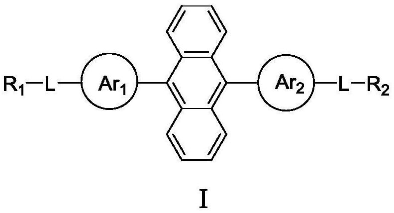
A compound and anthracene-based technology, applied in the field of organic electroluminescence, can solve problems such as obvious crystallinity and aggregation tendency, affect device performance, and poor batch stability, achieve good hole transport ability, improve luminous efficiency, and reduce preparation costs. cost effect
- Summary
- Abstract
- Description
- Claims
- Application Information
AI Technical Summary
Problems solved by technology
Method used
Image
Examples
preparation example Construction
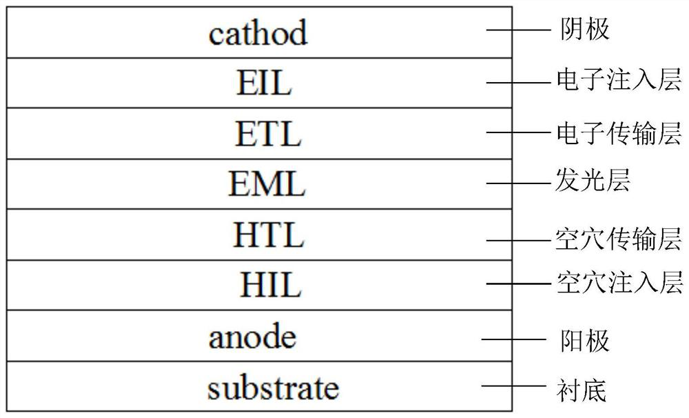
[0122] Preparation method of organic light emitting diode device:
[0123] (1) First, the ITO substrate was cleaned in the following order: 5% KOH solution ultrasonic for 15 min, pure water ultrasonic for 15 min, isopropanol ultrasonic for 15 min, oven drying for 1 h; then the substrate was transferred to UV-OZONE equipment for surface treatment for 15 min, treated Transfer to the glove box immediately after finishing.
[0124] (2) A layer of hole injection layer material, namely PEDOT:PSS film, was spin-coated on a clean ITO substrate, and then baked at 230 °C for 15 min. A layer of HTL layer thin film, namely VNPB, was spin-coated on the hole injection layer, and the thin film was baked at 200° C. for 30 min after spin-coating.
[0125] (3) A layer of HTL layer thin film, namely VNPB, was spin-coated on the hole injection layer, and the thin film was baked at 200° C. for 30 min after spin-coating.
[0126] (4) Dissolve the dendrimer compound with solvent o-xylene and prepa...
Embodiment 1
[0129] The organic light-emitting diode device 1 is prepared according to the structure and preparation method of the organic light-emitting diode device by using the compound M1 as the material of the light-emitting layer.
Embodiment 2~6
[0131] The organic light emitting diode devices 2 to 6 are respectively prepared according to the structure and preparation method of the organic light emitting diode device by using the compounds M2 to M6 as the light emitting layer material (M).
PUM
| Property | Measurement | Unit |
|---|---|---|
| thickness | aaaaa | aaaaa |
Abstract
Description
Claims
Application Information


