
Perovskite solar cell with hole transport system free of ionic additive
A technology of solar cells and hole transport layers, applied in circuits, electrical components, photovoltaic power generation, etc., can solve the problems of easy moisture absorption, damage to the lattice structure, affecting battery life, etc., to avoid the influence of water molecules and improve the device. Effects of stability, high hole mobility
- Summary
- Abstract
- Description
- Claims
- Application Information
AI Technical Summary
Problems solved by technology
Method used
Image

Examples
Embodiment 1
[0031] Example 1: Non-ionic additive perovskite solar cells prepared by solution method
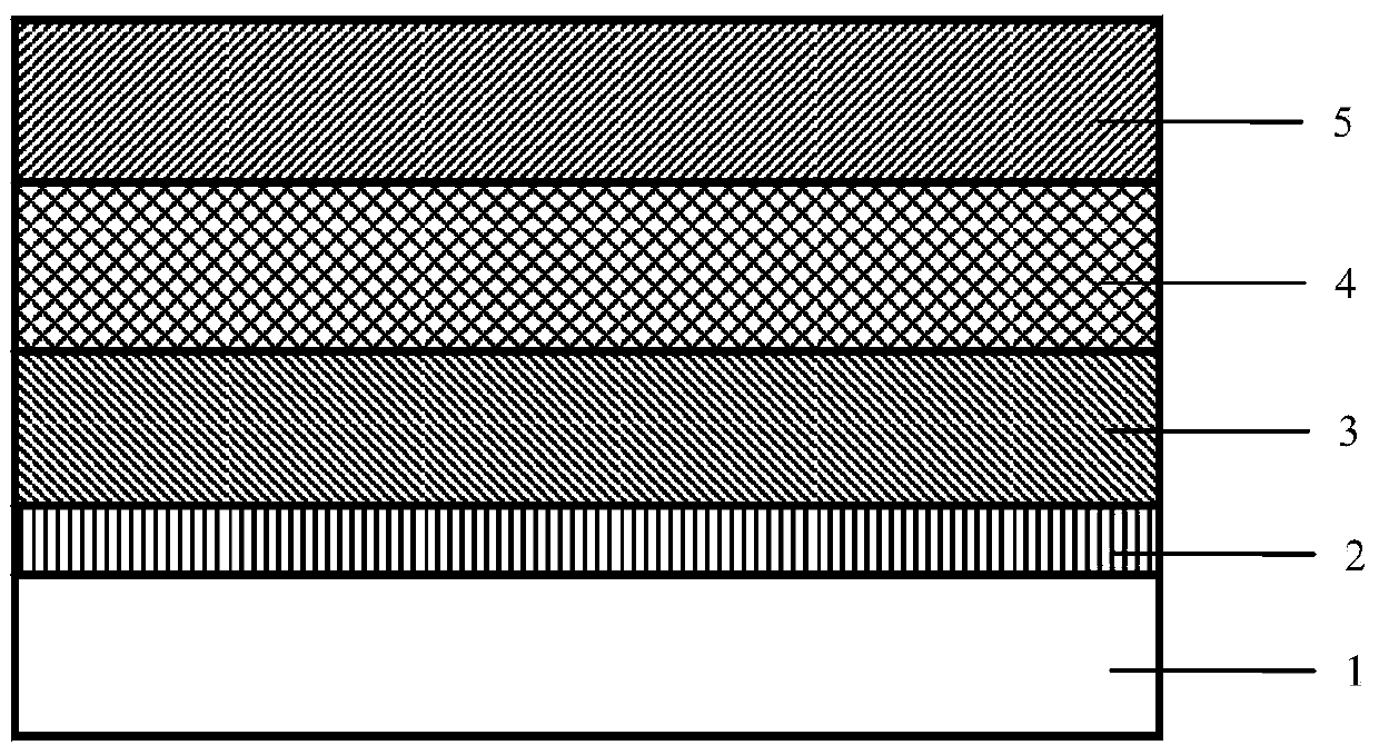
[0032] For the preparation of device functional layers, see figure 1 , mainly including various functional layers stacked on the substrate and the transparent electrode 1 : electron transport layer 2 , light absorbing layer 3 , hole transport layer 4 , and metal electrode 5 . The preparation process is as follows:
[0033] 1) FTO conductive glass is used as the substrate and transparent electrode 1, with a thickness of 2-5 mm and a surface resistance of less than 50 ohms;
[0034]2) Coat the substrate and the transparent electrode 1 with a 0.15-0.3 M bis(acetylacetonate) diisopropyl titanate (titaniumdiisopropoxidebis(acetylacetonate)) precursor solution by spin coating method, and place it in a muffle furnace at 350 ℃~500℃ high temperature sintering for 30min~90min to obtain TiO with a thickness of about 10~100nm 2 Dense film as electron transport layer 2;
[0035] 3) The light-absor...
Embodiment 2
[0045] Embodiment 2: there is non-ionic additive perovskite solar cell prepared by evaporation method
[0046] For the preparation of device functional layers, see figure 1 , mainly including various functional layers stacked on the substrate and the transparent electrode 1 : electron transport layer 2 , light absorbing layer 3 , hole transport layer 4 , and metal electrode 5 . The preparation process is as follows:
[0047] 1) FTO conductive glass is used as the substrate and transparent electrode 1, with a thickness of 2-5 mm and a surface resistance of less than 50 ohms;
[0048] 2) Coat the substrate and the transparent electrode 1 with a 0.15-0.3 M bis(acetylacetonate) diisopropyl titanate (titaniumdiisopropoxidebis(acetylacetonate)) precursor solution by spin coating method, and place it in a muffle furnace at 350 ℃~500℃ high temperature sintering for 30min~90min to obtain TiO with a thickness of about 10~100nm 2 Dense film as electron transport layer 2;
[0049] 3) ...
PUM
| Property | Measurement | Unit |
|---|---|---|
| thickness | aaaaa | aaaaa |
| thickness | aaaaa | aaaaa |
| thickness | aaaaa | aaaaa |
Abstract
Description
Claims
Application Information