Meta-surface terahertz broadband absorber with metal-medium-graphene structure

A graphene and metasurface technology, applied in the direction of instruments, optics, electrical components, etc., can solve the problems that hinder the development of applications and cannot be tuned, and achieve the effect of wide absorption bandwidth and wide-angle incident absorptivity

Pending Publication Date: 2021-02-05
SOUTH CHINA NORMAL UNIVERSITY
View PDF0 Cites 4 Cited by
  • Summary
  • Abstract
  • Description
  • Claims
  • Application Information

AI Technical Summary

Problems solved by technology

However, once the characteristics of the existing traditional absorbers are determined, they are non-tunable, which greatly hinders their application in society (Kim J, Han K, Hahn J W, et al. Selective dual-band metamaterial perfect absorber for infrared stealthtechnology.(Scientific Reports)Landy N I,Sajuyigbe S,Mock J J,et al.Perfect Metamaterial Absorber.(Physical Review Letters)Liu N,Mesch M,Weiss T,etal.Infrared perfect absorber and its application as plasmonic sensor.[J].(Nano Letters))

Method used


Image

  • Meta-surface terahertz broadband absorber with metal-medium-graphene structure
  • Meta-surface terahertz broadband absorber with metal-medium-graphene structure
  • Meta-surface terahertz broadband absorber with metal-medium-graphene structure

Examples


Embodiment

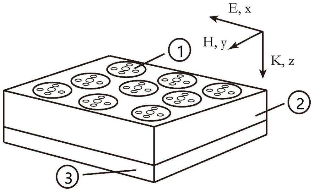
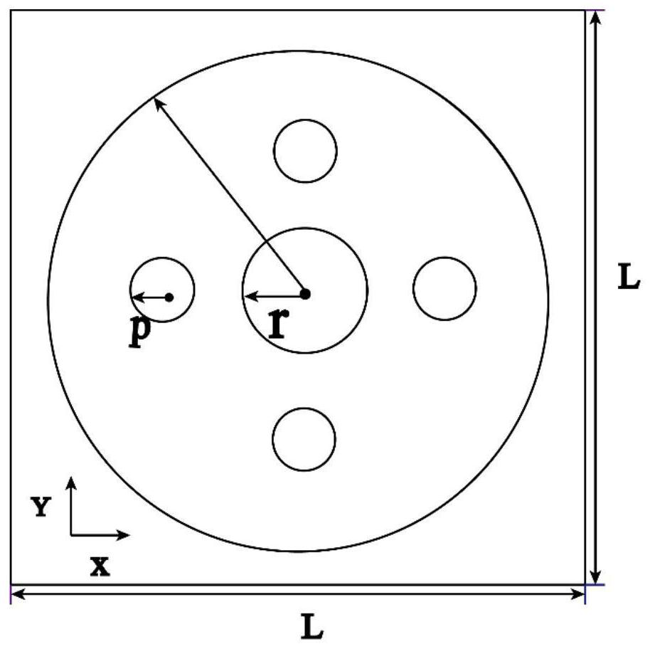
[0025] A metal-dielectric-graphene-structured metasurface terahertz broadband absorber, such as figure 1 As shown, it includes a metal reflective layer 3, an intermediate dielectric interlayer 2 and a patterned graphene structure; wherein, the patterned graphene structure includes several metasurface patterned graphene periodic units 1;

[0026] Several metasurface patterned graphene periodic units 1 are periodically arranged on the upper surface of the intermediary interlayer 2 to form a coplanar layer, and the metal reflective layer 3 is closely attached to the lower surface of the intermediary interlayer 2;

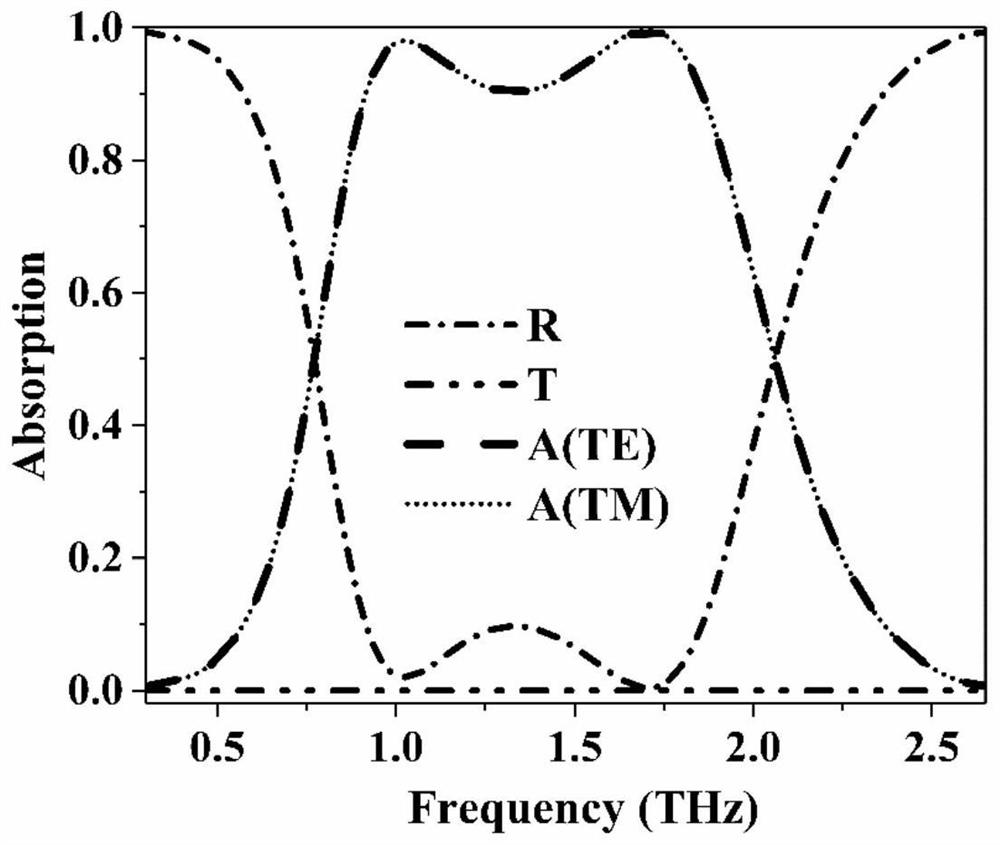
[0027] The terahertz plane wave light source is vertically irradiated on the patterned graphene structure, and a section of absorption broadband is obtained to realize broadband absorption. The Fermi level of graphene in the structure is adjusted by changing the side gate voltage. When the side gate voltage is energized, Change the Fermi level of graphene, and then rea...


PUM

PropertyMeasurementUnit
lengthaaaaaaaaaa
widthaaaaaaaaaa
thicknessaaaaaaaaaa

Abstract

The invention discloses a metasurface terahertz broadband absorber of a metal dielectric graphene structure. The broadband absorber comprises a metal reflection layer, an intermediate medium interlayer and a patterned graphene structure. The patterned graphene structure comprises a plurality of metasurface patterned graphene periodic units; the plurality of metasurface patterned graphene periodicunits are periodically arranged on the upper surface of the intermediate medium interlayer to form a coplanar layer, and the metal reflecting layer is tightly attached to the lower surface of the intermediate medium interlayer; the terahertz plane wave light source vertically irradiates the patterned graphene structure to obtain a section of absorption broadband, broadband absorption is achieved,the Fermi level of graphene in the patterned graphene structure is adjusted by changing the side end gate voltage, and the Fermi level of graphene is changed under the condition that the side end gatevoltage is powered on; therefore, the dynamic adjustment of the absorption level based on the graphene broadband absorber is realized. The invention has the characteristics of wide absorption bandwidth, wide-angle incidence, adjustable absorptivity and the like.

Description

technical field [0001] The invention relates to the field of optical devices based on a metal-medium-graphene structure metasurface, in particular to a metal-medium-graphene structure metasurface terahertz broadband absorber. Background technique [0002] In recent years, terahertz (THz) waves are located between microwaves and infrared light in the electromagnetic spectrum. Due to its important research value and broad development prospects in communication, imaging, sensing detection and spectroscopy, it has attracted great attention from researchers. Nowadays, with the in-depth research on terahertz technology, the demand for terahertz photonic devices such as filters, polarization converters, absorbers, etc. is becoming more and more urgent. Among these photonic devices, terahertz absorbers are also receiving more and more attention because of their great research value and potential applications. However, once the characteristics of the existing traditional absorbers ...

Claims


Application Information

Patent Timeline
Patent Type & Authority Applications(China)
IPC IPC(8): H01Q17/00H01Q15/00G02B5/00
CPCG02B5/003H01Q15/0086H01Q17/008
Inventor 蒙红云沈鸿洋刘凤祥谭春华黄旭光
Owner SOUTH CHINA NORMAL UNIVERSITY
Why Eureka
Try Eureka