A metal/dielectric ultra-broadband absorption film and its preparation method

An absorption film and ultra-broadband technology, which is applied in the field of metal/dielectric ultra-broadband absorption film and its preparation, can solve the problems of not reaching the absorption threshold, limiting the application range, and narrow absorption bandwidth, so as to increase adhesion and firmness, broaden the Application range and the effect of widening the absorption bandwidth

Active Publication Date: 2020-07-28
TONGJI UNIV
View PDF5 Cites 0 Cited by
  • Summary
  • Abstract
  • Description
  • Claims
  • Application Information

AI Technical Summary

Problems solved by technology

However, there are defects in these two film structures: first, the problem of metal selection is not solved, and the use of Ni or Ti as the absorbing metal cannot reach the absorption threshold of this structure, resulting in a narrow absorption bandwidth; second, the use of metal Ni is used as a substrate, which limits its application range as an absorber, and Ti is used as a metal substrate for a thin film, which reduces the adhesion and firmness between the thin film and the substrate, and limits its film-forming quality.

Method used


Image

  • A metal/dielectric ultra-broadband absorption film and its preparation method
  • A metal/dielectric ultra-broadband absorption film and its preparation method
  • A metal/dielectric ultra-broadband absorption film and its preparation method

Examples


preparation example Construction

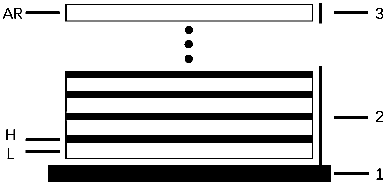
[0039] The preparation method of the above-mentioned metal / dielectric ultra-broadband absorption film includes: the determination of the number of layers of the metal / dielectric film stack; the selection of the material and film thickness of the low refractive index medium film layer L; the high absorption metal thin layer The selection of the metal material and film thickness of H; the selection of the material and film thickness of the single-layer low refractive index medium anti-reflection film AR.

[0040] The metal / dielectric ultra-broadband absorption film designed by the invention can realize wider absorption bandwidth, more stable film structure and wider application range.

Embodiment 1

[0042]In the metal / dielectric ultra-broadband absorption film provided in this embodiment, the first film structure is (LH) n1 . Since the approximate absorptivity of the film is A=1-R-T, in order to fully absorb the film system and at the same time suppress the incident light from passing through the film system to the greatest extent, the transmittance of the film system must be T=0, and n1 needs to be greater than 30, which is taken in this embodiment n1=30. At this time, the structure of the entire metal / dielectric ultra-broadband absorbing film is defined as: JGS1|(LH) 30 |Air.

[0043] In order to make the preparation of the metal / dielectric ultra-broadband absorption film more precise, the low-refractive index dielectric film layer L can choose SiO with a relatively mature preparation process. 2 . At the same time, in this metal / dielectric structured film system, the position of the first-order Bragg reflection peak is determined by the thickness of the medium d=λ / 2...


PUM

PropertyMeasurementUnit
thicknessaaaaaaaaaa
thicknessaaaaaaaaaa

Abstract

The invention relates to a metal / dielectric ultra-wideband absorbing film. The metal / dielectric ultra-wideband absorbing film comprises a substrate, a first film and a second film which are sequentially disposed from bottom to top, the first film (2) is a metal / dielectric film stack formed by alternately arranging low-refractive index dielectric films L and high-absorption metal films H, and one side, in contact with the substrate, of the first film is the low-refractive index dielectric film L, and the second film is a single-layer low-refractive index dielectric antireflection film AR. Compared with the prior art, the method omits a traditional thick-layer precious metal substrate, increases the adhesion and the firmness between the film and the substrate, adopts a novel material selection process, realizes an absorption bandwidth of about 7 [mu]m at 400-7000 nm, and makes the obtained film have an average absorption rate of above 92%.

Description

technical field [0001] The invention relates to an optical thin film, in particular to a metal / dielectric ultra-broadband absorption thin film and a preparation method thereof. Background technique [0002] Broadband absorbing thin films have a wide range of applications in photovoltaic cells, photoelectric detection, optical filters, invisibility technology, thermal light source radiation and other fields. Its absorption bandwidth is a key factor affecting its system performance. [0003] At present, there are three main technical approaches to realize broadband absorption films: microstructure films, high absorption black films, and metal / dielectric composite films. Among them, although the microstructured film can achieve broadband absorption, it requires precise etching technology, the preparation process is relatively complicated, and the preparation cost is high, which is not conducive to large-scale industrial production; and for large-sized optical components, the m...

Claims


Application Information

Patent Timeline
Patent Type & Authority Patents(China)
IPC IPC(8): B32B9/00B32B9/04B32B15/00B32B27/36B32B27/06B32B37/00
CPCB32B9/00B32B9/002B32B9/04B32B9/041B32B15/00B32B27/06B32B27/36B32B37/00B32B2307/41B32B2311/00B32B2367/00
Inventor 焦宏飞钮信尚张学敏马彬张锦龙程鑫彬王占山
Owner TONGJI UNIV
Why Eureka
Try Eureka