An input buffer circuit and memory

An input buffer circuit and input buffer technology, applied in the storage field, can solve problems such as abnormal output of the clock logic signal ICK, and achieve the effects of avoiding abnormal status, ensuring normal operation, and filtering noise

Active Publication Date: 2022-06-21
WUHAN XINXIN SEMICON MFG CO LTD
View PDF8 Cites 0 Cited by
  • Summary
  • Abstract
  • Description
  • Claims
  • Application Information

AI Technical Summary

Problems solved by technology

That is, during the rising and falling processes of the clock input signal CLK, the clock conversion is performed one more time respectively, so that the output of the clock logic signal ICK is abnormal.

Method used


Image

  • An input buffer circuit and memory
  • An input buffer circuit and memory
  • An input buffer circuit and memory

Examples


Embodiment Construction

[0026] The technical solutions in the embodiments of the present application will be clearly and completely described below with reference to the accompanying drawings in the embodiments of the present application. Obviously, the described embodiments are only a part of the embodiments of the present application, but not all of the embodiments. Based on the embodiments in the present application, all other embodiments obtained by those skilled in the art without creative work fall within the protection scope of the present application. The same or similar reference numbers throughout the embodiments denote the same or similar elements or elements having the same or similar functions.

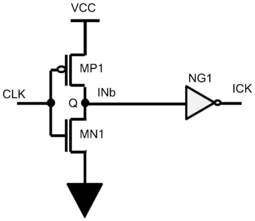
[0027] see Figure 4 , a schematic diagram of the structure of the input buffer circuit provided according to the first embodiment of the present application. like Figure 4 As shown, the shown input buffer circuit 40 includes: a first input buffer unit 41 , a second input buffer unit 42 , an...


PUM


Abstract

The application discloses an input buffer circuit and a memory. The input buffer circuit of this application, by configuring the input high voltage threshold to be different from the input low voltage threshold, when the input signal is between the input high voltage threshold and the input low voltage threshold, the logic output signal does not perform state switching, thereby eliminating noise on the input signal interference. That is, the present application can filter out the noise in the input signal, avoid the abnormal state of the logic output signal corresponding to the input signal, and ensure the normal operation of the device.

Description

technical field [0001] The present application relates to the field of storage technologies, and in particular, to an input buffer circuit and a memory capable of filtering out noise. Background technique [0002] An input buffer is an indispensable basic block in an integrated circuit, and it can be configured to perform voltage detection for a threshold voltage in order to confirm whether the voltage of the input signal is higher or lower than the threshold voltage. An input buffer consisting of CMOS-based logic devices is typically configured to receive a high or low voltage signal from a peripheral and then provide a logic state corresponding to the high or low signal. When the voltage of the input signal is higher than the threshold voltage, the output logic level changes from low to high; when the voltage of the input signal is lower than the threshold voltage, the output logic level changes from high to low. [0003] In a serial peripheral interface (Serial Periphera...

Claims


Application Information

Patent Timeline
Patent Type & Authority Patents(China)
IPC IPC(8): G11C16/10G11C16/06H03K19/003
CPCG11C16/10G11C16/06H03K19/00315H03K19/00361H03K19/00307H03K19/00346H03K19/00353
Inventor 郑钟倍
Owner WUHAN XINXIN SEMICON MFG CO LTD
Why Eureka
Try Eureka