

Edge-emitting semiconductor laser and preparation method thereof
A technology of semiconductors and lasers, applied in the field of lasers, can solve the problems of high cost and poor stability of the external cavity collimation scheme, and achieve the effect of improving integration and stability
- Summary
- Abstract
- Description
- Claims
- Application Information
AI Technical Summary
Problems solved by technology
Method used
Image

Examples
Embodiment Construction
[0034] In order to make the objectives, technical solutions and advantages of the present invention clearer, the present invention will be further described in detail below with reference to the accompanying drawings and embodiments. It should be understood that the specific embodiments described herein are only used to explain the present invention, but not to limit the present invention. In addition, the technical features involved in the various embodiments of the present invention described below can be combined with each other as long as they do not conflict with each other.
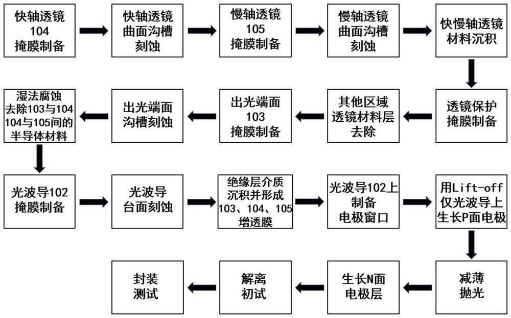
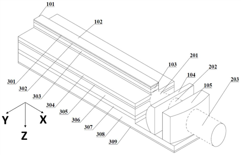
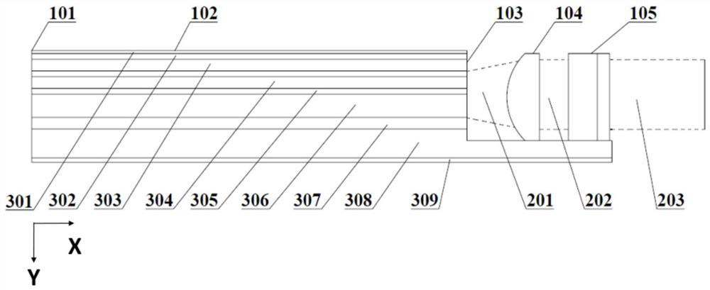
[0035] like figure 1 As shown, the manufacturing process of the edge-emitting semiconductor laser according to the embodiment of the present invention is as follows:
[0036] Step 1: Make an epitaxial wafer.
[0037] In some embodiments, the epitaxial wafer includes an N-type doped substrate and a stack disposed on the substrate. The plane where the substrate is located is defined as the X-Y plan...
PUM
 Abstract
Description
Claims
Application Information