Integrated packaging device for surface-mounted diode

A technology for packaging devices and diodes, applied in semiconductor devices, semiconductor/solid-state device manufacturing, electrical components, etc., can solve problems such as inability to connect to the next process, inability to connect to lead frames, and unsatisfactory methods, so as to achieve rapid action and ensure efficiency , the effect of improving production efficiency

Active Publication Date: 2021-02-12
四川晶辉半导体有限公司
View PDF6 Cites 7 Cited by
  • Summary
  • Abstract
  • Description
  • Claims
  • Application Information

AI Technical Summary

Problems solved by technology

[0003] In order to improve production efficiency, it is necessary to use a conveying mechanism to transport the lead frame as a carrier so that each process point can be connected in series. However, the existing method is not ideal, and there are still relatively independent modes between processes, especially In the co

Method used


Image

  • Integrated packaging device for surface-mounted diode
  • Integrated packaging device for surface-mounted diode
  • Integrated packaging device for surface-mounted diode

Examples


Embodiment

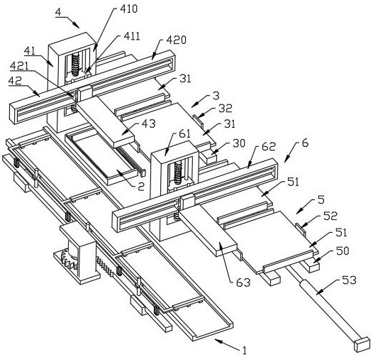
[0047] This example provides a chip diode lead frame delivery device, including: a delivery mechanism, a glue tank, a first stroke mechanism, a jumper carrying mechanism, a first stroke mechanism, and the like.

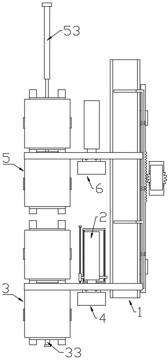
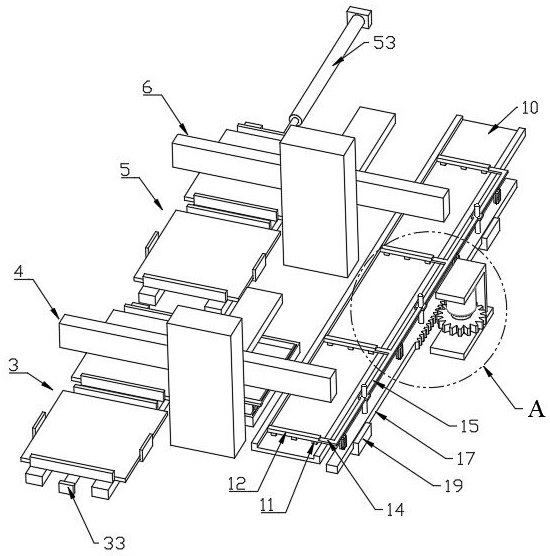
[0048] Specifically, such as Figure 1~3 Shown:

[0049] The conveying mechanism 1 is used for conveying the lead frame; the glue tank 2 is arranged on one side of the conveying mechanism 1 in the length direction to provide glue / colloid. The chip carrying mechanism 3 is located on the outside of the glue tank 2, and includes a first bracket 30, two sets of first four-way limiting plates 32 formed on the first bracket 30, and a A chip template 31, the chip template 31 carries a chip.

[0050]The first stroke mechanism 4 is located at one end of the glue tank 2, and includes a first elevating mechanism 41, a first horizontal linear mechanism 42 disposed on the first elevating mechanism 41, and a sticky core plate 43 disposed on the first horizontal linear mechanism 4...


PUM


Abstract

The invention discloses an integrated packaging device for a surface-mounted diode. The device comprises a conveying mechanism; a glue groove which is arranged on one side of the conveying mechanism in the length direction; a chip bearing mechanism which comprises a first bracket and two groups of first four-way limiting plates formed on the first bracket, wherein a chip template is arranged between each group of first four-way limiting plates; a first stroke mechanism which is located at one end of the glue groove and comprises a first lifting mechanism, a first horizontal linear mechanism and a core adhering plate; a jump piece bearing mechanism which comprises a second bracket and two groups of second four-way limiting plates formed on the second bracket, wherein a jump piece template is arranged between each group of second four-way limiting plates; and a second stroke mechanism which comprises a second lifting mechanism, a second horizontal linear mechanism and a pneumatic suctioncup. By means of a core feeding mechanism, a jump piece pasting mechanism and the like which are arranged along a lead frame conveying line, the stepping type continuous conveying of lead frames is achieved, gluing, core pasting and core feeding can be efficiently completed, jump piece pasting can be completed in the conveying process, and the process efficiency is greatly improved.

Description

technical field [0001] The invention relates to the field of semiconductor components, in particular to ultra-thin chip diode packaging, and in particular to a chip diode integrated packaging device. Background technique [0002] The packaging process of ultra-thin SMD diodes includes steps such as die-attaching / adhesive / intimate, testing, patching / jumpering, welding, heating and curing. Generally, in order to meet the requirements of mass production and high-efficiency production, lead frames are used as carriers. . The lead frame array has multiple rows and columns of functional units, each unit is used to form an ultra-thin diode in the package. Finally, after the packaging is completed, the ribs are punched or cut to obtain a single independent device. [0003] In order to improve production efficiency, it is necessary to use a conveying mechanism to transport the lead frame as a carrier so that each process point can be connected in series. However, the existing metho...

Claims


Application Information

Patent Timeline
IPC IPC(8): H01L21/67H01L29/861
CPCH01L21/67121H01L29/861
Inventor 曾尚文陈久元杨利明李洪贞
Owner 四川晶辉半导体有限公司
Why Eureka
Try Eureka