Lead frame for chip packaging, preparation method thereof, and chip packaging structure

A lead frame and chip packaging technology, which is applied in semiconductor/solid-state device manufacturing, electrical components, electric solid-state devices, etc., can solve the problems of high cost, complex process, and difficulty in matching the thickness of filled electrophoretic resin, etc. Simple, low-prep effects

Pending Publication Date: 2021-02-12
深圳市鼎华芯泰科技有限公司
View PDF1 Cites 3 Cited by
  • Summary
  • Abstract
  • Description
  • Claims
  • Application Information

AI Technical Summary

Problems solved by technology

In this invention, electrophoretic resin is filled in the groove etched by copper foil as the substrate. The etching of copper foil needs to be covered with a photosensitive film. It is difficult to match the depth of copper foil groove etching with the thickness of filled electrophoretic resin. The fading performance of the electrophoresis layer has a greater impact, and the plating tank of the electrophoresis process requires strict maintenance, and the invention is complicated in process and high in cost.

Method used


Image

  • Lead frame for chip packaging, preparation method thereof, and chip packaging structure
  • Lead frame for chip packaging, preparation method thereof, and chip packaging structure
  • Lead frame for chip packaging, preparation method thereof, and chip packaging structure

Examples


Embodiment Construction

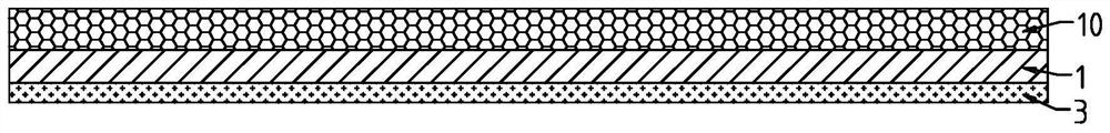
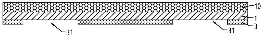
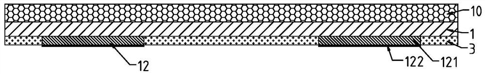
[0065] Embodiment 1 of the present invention is used for the structure of a unit circuit of a lead frame for chip packaging as follows: Figure 11 As shown, it includes a carrier sheet 2 , a solder resist ink layer 3 , two solder resist ink layers and a plurality of unit circuits arranged in a matrix. Each unit circuit includes two electrodes, and the electrodes include a top electrode 11 and a bottom electrode 12 . The top electrode 11 is arranged on the top surface of the solder resist ink layer 3 . Corresponding to each unit circuit, the solder resist ink layer 3 includes two bottom electrode holes 31 , the bottom electrode 12 is arranged in the bottom electrode holes 31 , and the top of the bottom electrode 12 is fixed on the bottom surface of the top electrode 11 . The carrier sheet 2 is peelably pasted on the solder resist ink layer 3 and the bottom surface of the bottom electrode 12 .

[0066] In this embodiment, the lateral dimension of the top electrode 11 is greater...


PUM


Abstract

The invention discloses a lead frame for chip packaging, a preparation method thereof, and a chip packaging structure. The lead frame comprises a bearing sheet, a first solder resist ink layer and a plurality of unit circuits arranged in a matrix, each unit circuit comprises a plurality of electrodes, and each electrode comprises a top electrode and a bottom electrode; the top electrodes are arranged on the top surface of the first solder resist ink layer; corresponding to each unit circuit, the first solder resist ink layer comprises a bottom electrode hole corresponding to the electrode, thebottom electrode is arranged in the bottom electrode hole, and the top of the bottom electrode is fixed on the bottom surface of the top electrode; and the bearing sheet is peelably adhered to the first solder resist ink layer and the bottom surface of the bottom electrode. The preparation method of the lead frame is few in steps, simple in process flow and low in cost.

Description

[technical field] [0001] The invention relates to chip packaging, in particular to a lead frame for chip packaging, a preparation method and a chip packaging structure. [Background technique] [0002] The main function of the lead frame is to provide a mechanically supported carrier for the chip, and to form an electrical signal path by connecting the chip circuit inside and outside as a conductive medium, and to dissipate the heat generated by the chip together with the package shell. [0003] The invention with application number CN202010538887.5 discloses a lead frame for chip packaging and a preparation method. The lead frame includes a substrate, a base island, and a plurality of pins arranged around the periphery of the base island. The base island includes an upper base island arranged above the substrate, a lower base island arranged below the substrate, and a penetrating substrate, connecting the upper base island and the lower base island. The metal island of the ...

Claims


Application Information

Patent Timeline
Patent Type & Authority Applications(China)
IPC IPC(8): H01L23/495H01L21/48H01L33/62H01L23/31
CPCH01L21/4821H01L21/4828H01L23/3107H01L23/49541H01L23/49548H01L33/62H01L2224/73265H01L2924/181H01L2924/00012
Inventor 何忠亮王成刘卫宾沈洁
Owner 深圳市鼎华芯泰科技有限公司
Why Eureka
Try Eureka