
Solder-free high-thermal-conductivity semiconductor substrate and preparation method thereof

A high thermal conductivity, semiconductor technology, applied in semiconductor lasers, structural details of semiconductor lasers, laser components, etc., can solve problems such as high thermal resistance, chip breakage and damage, and reduced chip life.

Inactive Publication Date: 2020-04-28
CHANGCHUN UNIV OF SCI & TECH
View PDF2 Cites 2 Cited by
  • Summary
  • Abstract
  • Description
  • Claims
  • Application Information

AI Technical Summary

Problems solved by technology

If the excessive heat cannot be dissipated in time, the stress between the chip and the solder will increase, and in severe cases, the chip will be broken and damaged, reducing the life of the chip
Moreover, the solder layer on the heat sink has strict requirements on temperature and pressure when packaging the device chip, which can easily cause damage to the back electrode of the device chip, resulting in poor ohmic contact and high thermal resistance.

Method used


Image

  • Solder-free high-thermal-conductivity semiconductor substrate and preparation method thereof
  • Solder-free high-thermal-conductivity semiconductor substrate and preparation method thereof

Examples


preparation example Construction

[0023] The invention provides a method for preparing a solder-free high thermal conductivity semiconductor substrate, comprising the following steps:

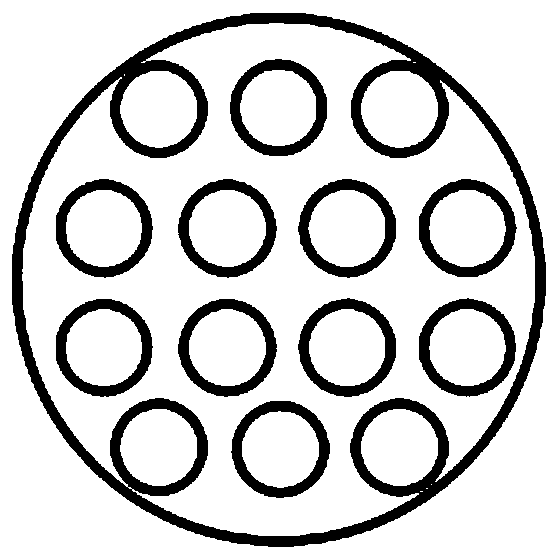
[0024] performing a photolithography process on the back of the substrate, forming a pattern of holes arranged in periodic distribution on the back of the substrate to obtain a photolithographic substrate;

[0025] performing an etching process on the photolithographic substrate sheet, forming periodically distributed holes on the back of the photolithographic substrate sheet to obtain an etched substrate;

[0026] Filling the holes of the etched substrate with a metal material by evaporation until the metal material is flush with the back of the etched substrate, and then continuing to form a metal material layer on the back of the etched substrate by evaporation to obtain Solder-free high thermal conductivity semiconductor substrate.

[0027] Since the size of the semiconductor laser is in the micron level, fine dust will al...

Embodiment 1

[0050] Using GaAs as a substrate and silver nanowires as an elastic filling material to prepare a solder-free high thermal conductivity semiconductor substrate includes the following steps:

[0051] (1) Photolithography: ultrasonically clean the GaAs substrate with acetone, ethanol and deionized water for 15 minutes respectively, then dry it with nitrogen, and finally heat it on a heating plate at 100°C for 5 minutes to completely remove water vapor; Use hexamethyldisilazane (HMDS) to pretreat the cleaned GaAs substrate, and then use AZ5214 photoresist as a mask to uniform the back of the GaAs substrate, and set the speed of the uniform equipment to 4000r / min, the hold time is 35s, so that the thickness of the photoresist on the GaAs substrate is 1.5μm; place the uniformed GaAs substrate on a heating platform with a temperature of 100°C, and soft bake for 90s; The soft-baked GaAs substrate was subjected to contact exposure, and the exposure time was 20s; the exposed GaSb subs...


PUM

PropertyMeasurementUnit
thicknessaaaaaaaaaa
thicknessaaaaaaaaaa
depthaaaaaaaaaa

Abstract

The invention provides a solder-free high-thermal-conductivity semiconductor substrate and a preparation method thereof, and belongs to the technical field of semiconductors. According to the semiconductor substrate is prepared by the method provided by the invention, holes are formed in the back surface, and filled with a metal material with relatively high ductility through an evaporation method; after the holes are filled, a metal material layer is then prepared on the back surface of the etched substrate by utilizing the evaporation method; when the semiconductor substrate is used, the metal material layer can be used as a solder layer, after the heat sink is heated, direct adhesion of the semiconductor substrate and the heat sink can be realized, an extra process of preparing the solder layer on the heat sink is omitted, and device preparation process steps are reduced. Besides, the holes are formed in the back surface of the substrate base body, and the holes are filled with themetal materials with good ductility and high heat conduction capability, so that the problems of chip damage and separation from the heat sink due to excessive stress when the chip is heated to expandare solved, the service life of the semiconductor laser chip is prolonged, and the performance of the semiconductor laser is improved.

Description

technical field [0001] The invention relates to the technical field of new substrate materials, in particular to a solder-free high thermal conductivity semiconductor substrate and a preparation method thereof. Background technique [0002] Optoelectronic devices are various functional devices made using the electro-photon conversion effect. Optoelectronic devices are the key and core components of optoelectronic technology, the frontier research field of modern optoelectronic technology and microelectronic technology, and an important part of information technology. Semiconductor laser is one of the most important devices in optoelectronic devices. It has developed rapidly since its birth. Because of its advantages such as high photoelectric conversion efficiency, wide coverage wavelength range, long service life, small size, light weight, and direct modulation, it has been widely used. Used in material processing, military, industrial, medical, communication and other fie...

Claims


Application Information

Patent Timeline
Patent Type & Authority Applications(China)
IPC IPC(8): H01S5/02H01S5/024
CPCH01S5/0207H01S5/024H01S5/02469
Inventor 魏志鹏唐吉龙申琳宿世臣张贺王海珠房丹王登魁王晓华马晓辉
Owner CHANGCHUN UNIV OF SCI & TECH
Learn More