Check patentability & draft patents in minutes with Patsnap Eureka AI!

CMOS image sensor pixel structure based on bionic vision

An image sensor and pixel structure technology, which is applied in image communication, color TV parts, TV system parts, etc., can solve the problem that CMOS image sensors cannot obtain black and white image signals and color image signals at the same time, so as to eliminate reset Noise, high research value and development prospects, effect of gain enhancement

Pending Publication Date: 2021-02-26
DALIAN UNIV OF TECH
View PDF0 Cites 1 Cited by
  • Summary
  • Abstract
  • Description
  • Claims
  • Application Information

AI Technical Summary

Problems solved by technology

[0004] The present invention mainly solves the technical problem that black-and-white image signals and color image signals cannot be simultaneously obtained on the CMOS image sensor of the prior art, and proposes a CMOS image sensor pixel structure based on bionic vision to obtain high sensitivity in the same CMOS image sensor respectively black and white image signal and color image signal

Method used


Image

  • CMOS image sensor pixel structure based on bionic vision
  • CMOS image sensor pixel structure based on bionic vision
  • CMOS image sensor pixel structure based on bionic vision

Examples


Embodiment Construction

[0030] In order to make the technical problems solved by the present invention, the technical solutions adopted and the technical effects achieved clearer, the present invention will be further described in detail below in conjunction with the accompanying drawings and embodiments. It should be understood that the specific embodiments described here are only used to explain the present invention, but not to limit the present invention. In addition, it should be noted that, for the convenience of description, only parts related to the present invention are shown in the drawings but not all content.

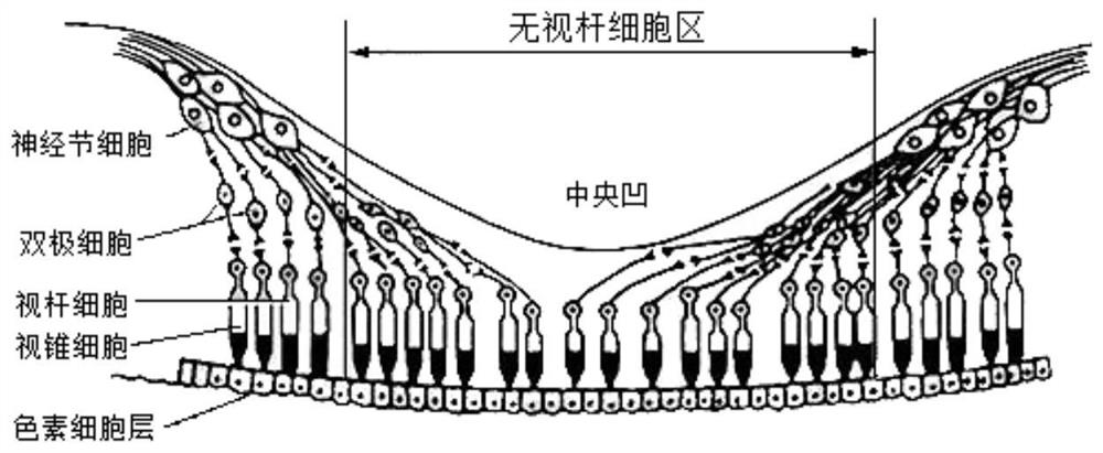
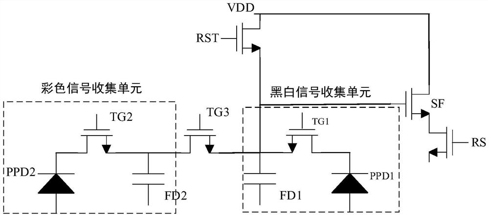
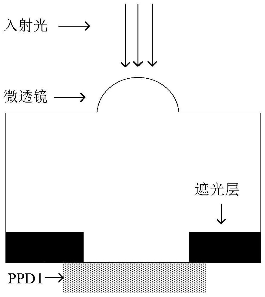
[0031] The CMOS image sensor pixel structure based on bionic vision provided by the embodiment of the present invention is designed based on the principle of bionic vision, and the human eye can be regarded as an image sensor with up to 576 million pixels. Such as figure 1 As shown, the human eye perceives external light signals through two types of visual cells, cone cells and ro...


PUM


Abstract

The invention relates to the technical field of CMOS image sensors, and provides a CMOS image sensor pixel structure based on bionic vision. The structure comprises a color signal collection unit, a black and white signal collection unit, a third transfer transistor TG3, a reset transistor RST, a source follower SF and a row selection transistor RS; the black and white signal collection unit comprises a first clamping photodiode PPD1, a first transfer transistor TG1 and a first floating diffusion capacitor FD1; and the color signal collection unit comprises a second clamping photodiode PPD2, asecond transfer transistor TG2 and a second floating diffusion capacitor FD2. According to the CMOS image sensor pixel structure of the invention, high-sensitivity black and white image signals and color image signals can be respectively obtained in the same CMOS image sensor.

Description

technical field [0001] The invention relates to the technical field of CMOS image sensors, in particular to a bionic vision-based CMOS image sensor pixel structure. Background technique [0002] With the rapid development of semiconductor technology, the application range of CMOS image sensors has been expanded to the fields of smart cars, monitoring and security, machine vision and consumer products. Especially in low-light imaging applications, parameters such as full well capacity, noise, dynamic range, sensitivity, and signal-to-noise ratio will directly affect the imaging effect. In order to improve the imaging performance of the camera in the low-light environment, an image processing technology for dark field enhancement is realized by weighting the dark field black-and-white image and the dark field color image. [0003] At present, in order to obtain a high-responsive black-and-white image and a color image, a combination of a color camera and a black-and-white cam...

Claims


Application Information

Patent Timeline
IPC IPC(8): H01L27/146H04N5/374
CPCH01L27/14609H01L27/14612H01L27/14645H04N25/76Y02D10/00
Inventor 曲杨常玉春梁红伟刘岩娄珊珊钟国强程禹宋辰昱曹伉
Owner DALIAN UNIV OF TECH
Features
  • R&D
  • Intellectual Property
  • Life Sciences
  • Materials
  • Tech Scout
  • Unparalleled Data Quality
  • Higher Quality Content
  • 60% Fewer Hallucinations
Learn More