A Y-shaped grid structure based on carbon-based materials and its preparation method

A carbon-based material and gate structure technology, which is applied in semiconductor/solid-state device manufacturing, semiconductor devices, electrical components, etc., can solve the problem of reducing the distance between source and drain electrodes and gate, unable to prepare short-channel transistors, and increasing device parasitics. effects and other issues, to achieve the effects of reducing parasitic effects, suppressing short-channel effects, and reducing power consumption

Active Publication Date: 2021-11-19
BEIJING INST OF CARBON BASED INTEGRATED CIRCUIT +2
View PDF10 Cites 0 Cited by
  • Summary
  • Abstract
  • Description
  • Claims
  • Application Information

AI Technical Summary

Problems solved by technology

T-gate devices have two structures, one is the gate-first self-aligned structure, its disadvantage is that the length of the channel defined by the self-aligned source-drain electrodes depends on the length of the gate cap, so in a long gate cap (larger Under the design of gate cap cross-sectional area and smaller gate resistance), short-channel transistors cannot be fabricated, and short channels are necessary for RF devices
The second is the gate-last non-self-aligned structure. Through two exposures, the complexity of the process is increased. Although the former problem can be solved, the distance between the source-drain electrode and the gate is reduced, thereby increasing the device size. Parasitic effects, which are detrimental to the high frequency performance of the device

Method used


Image

  • A Y-shaped grid structure based on carbon-based materials and its preparation method
  • A Y-shaped grid structure based on carbon-based materials and its preparation method
  • A Y-shaped grid structure based on carbon-based materials and its preparation method

Examples


Embodiment Construction

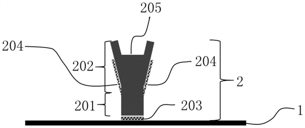
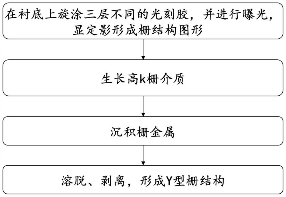
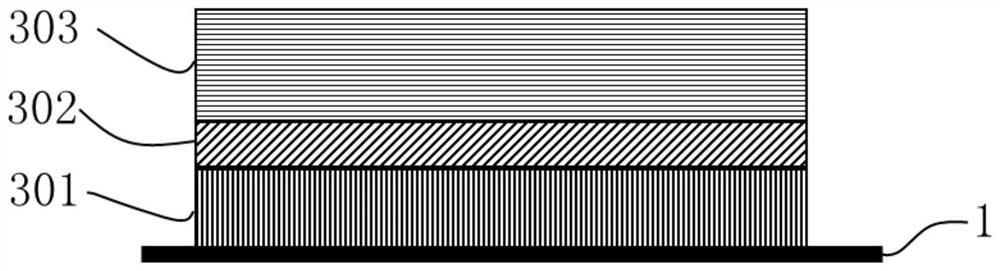
[0041]Embodiments of the present invention will be described in detail below with reference to the accompanying drawings. In the various drawings, the same elements are denoted by the same reference numerals, and various parts in the drawings are not drawn to scale. Also, some well-known parts may not be shown. For the sake of simplicity, the semiconductor structure obtained after several steps can be described in one figure.

[0042] It should be understood that when describing the structure of a device, when a layer or a region is referred to as being "on" or "over" another layer or another region, it may mean being directly on another layer or another region, or Other layers or regions are also included between it and another layer or another region. And, if the device is turned over, the layer, one region, will be "below" or "beneath" the other layer, another region.

[0043] The terms used in the present invention are for describing specific embodiments only, and are n...


PUM

PropertyMeasurementUnit
thicknessaaaaaaaaaa
thicknessaaaaaaaaaa

Abstract

The invention discloses a Y-shaped grid structure based on carbon-based materials, including a substrate of a carbon-based material channel layer, on which there is an integrated grid metal structure composed of a grid metal grid root and a grid metal grid cap, There is a first high-K gate dielectric layer between the gate metal structure and the carbon-based material channel layer, the lower part of the gate metal cap has a first width, and the upper part has a width greater than or equal to the first width. In the second width, two side surfaces are formed between the upper part and the lower part of the gate metal cap, and the second high-K gate dielectric layer is coated on the side surfaces respectively. At the same time, the preparation method of the Y-shaped gate structure is also proposed, which can form a self-aligned Y-shaped gate structure with only one exposure, and the process is simple and the operation is convenient. The Y-shaped gate structure based on carbon-based materials proposed by the present invention can further reduce parasitic effects while reducing gate resistance, and can improve the performance of carbon-based high-speed and high-frequency devices.

Description

technical field [0001] The invention relates to the technical field of transistor electronic device preparation, in particular to a carbon-based material-based Y-shaped gate structure and a preparation method thereof. Background technique [0002] Carbon-based electronic materials represented by three-dimensional material diamond, two-dimensional material graphene and quasi-one-dimensional material carbon nanotubes have ultra-wide bandgap, ultra-high carrier mobility, excellent thermal conductivity and mechanical properties, respectively. As well as the various quantum effects brought by the unique low-dimensional structure, it has great potential in the fields of radio frequency high-power, high-linearity, terahertz and photoelectric mixing devices. With the development of carbon-based radio frequency devices, the existing experimental results show that the performance of carbon-based radio frequency devices is still lagging behind theoretical expectations due to limitation...

Claims


Application Information

Patent Timeline
Patent Type & Authority Patents(China)
IPC IPC(8): H01L29/423H01L21/28
CPCH01L21/28008H01L29/42356H01L29/4236H01L29/42376
Inventor 周简硕丁力彭练矛
Owner BEIJING INST OF CARBON BASED INTEGRATED CIRCUIT
Why Eureka
Try Eureka