Method for improving electroplating hole filling process of circuit board
A technology for electroplating and filling holes and circuit boards. It is used in printed circuits, printed circuit manufacturing, electrical components and other directions. It can solve the problems of inability to fill holes with resin and the thinning process of grinding plates, and it is difficult to fill holes in the whole board, and achieve excellent hole filling. Effect, prevent filling holes, simple and easy-to-control effects
- Summary
- Abstract
- Description
- Claims
- Application Information
AI Technical Summary
Problems solved by technology
Method used
Image

Examples
Embodiment 1
[0039] A method for improving the electroplating hole filling process of a circuit board, comprising the steps of:
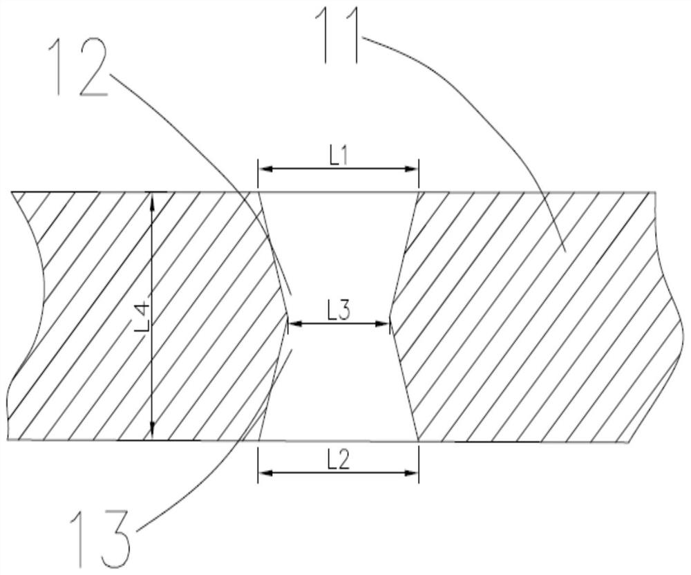
[0040] (1) Get the circuit board substrate 11 to be drilled, and use laser processing to drill the first hole 12 on the front of the circuit board substrate 11 and drill the second hole 13 in the corresponding circuit board substrate 11 back area; the first hole 12 communicate with the second channel 13 to form a through hole, and obtain a circuit board substrate 11 drilled with a through hole;
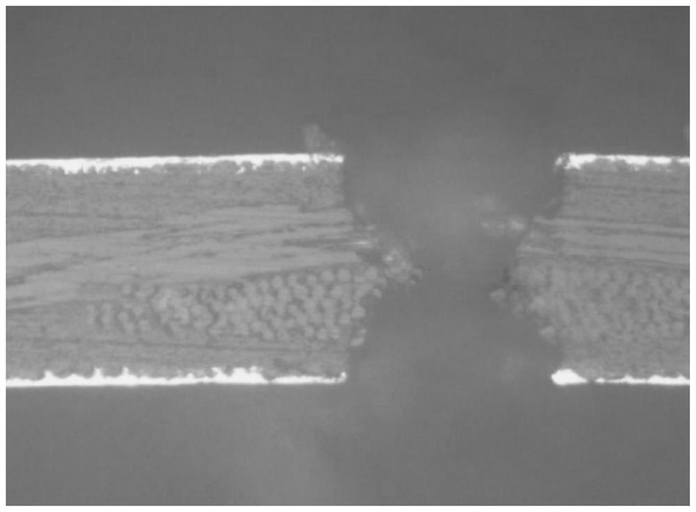
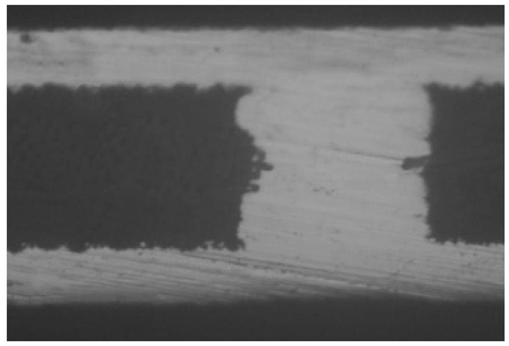
[0041] (2) Carry out copper electroplating and hole filling on the circuit board substrate 11 drilled with through holes.
[0042] Such as figure 1 As shown, in the step (1), the communication between the first channel 12 and the second channel 13 is funnel-shaped, and the thin ends of the first channel 12 and the second channel 13 are connected.
[0043] Further, in the step (1), the aperture of the opening of the first channel 12 located on the front of the circuit ...
Embodiment 2
[0053] A method for improving the electroplating hole filling process of a circuit board, comprising the steps of:
[0054] (1) Get the circuit board substrate 11 to be drilled, and use laser processing to drill the first hole 12 on the front of the circuit board substrate 11 and drill the second hole 13 in the corresponding circuit board substrate 11 back area; the first hole 12 communicate with the second channel 13 to form a through hole, and obtain a circuit board substrate 11 drilled with a through hole;
[0055] (2) Carry out copper electroplating and hole filling on the circuit board substrate 11 drilled with through holes.
[0056] Further, in the step (1), the communication between the first channel 12 and the second channel 13 is funnel-shaped, and the thin ends of the first channel 12 and the second channel 13 are connected. The invention adjusts the parameters of the laser drilling, adjusts the parameters of the laser drilling, makes the through hole form a funnel...
Embodiment 3
[0068] A method for improving the electroplating hole filling process of a circuit board, comprising the steps of:
[0069] (1) Get the circuit board substrate 11 to be drilled, and use laser processing to drill the first hole 12 on the front of the circuit board substrate 11 and drill the second hole 13 in the corresponding circuit board substrate 11 back area; the first hole 12 communicate with the second channel 13 to form a through hole, and obtain a circuit board substrate 11 drilled with a through hole;
[0070] (2) Carry out copper electroplating and hole filling on the circuit board substrate 11 drilled with through holes.
[0071] Further, in the step (1), the communication between the first channel 12 and the second channel 13 is funnel-shaped, and the thin ends of the first channel 12 and the second channel 13 are connected. The invention adjusts the parameters of the laser drilling, adjusts the parameters of the laser drilling, makes the through hole form a funnel...
PUM
| Property | Measurement | Unit |
|---|---|---|
| pore size | aaaaa | aaaaa |
| thickness | aaaaa | aaaaa |
| thickness | aaaaa | aaaaa |
Abstract
Description
Claims
Application Information
 - R&D
- Intellectual Property
- Life Sciences
- Materials
- Tech Scout
- Unparalleled Data Quality
- Higher Quality Content
- 60% Fewer Hallucinations
Browse by: Latest US Patents, China's latest patents, Technical Efficacy Thesaurus, Application Domain, Technology Topic, Popular Technical Reports.
© 2025 PatSnap. All rights reserved.Legal|Privacy policy|Modern Slavery Act Transparency Statement|Sitemap|About US| Contact US: help@patsnap.com