Laser annealing method and laser annealing system for power device

A power device, laser annealing technology, applied in the direction of semiconductor devices, semiconductor/solid-state device manufacturing, electrical components, etc.

Pending Publication Date: 2021-03-02
BEIJING U PRECISION TECH
View PDF0 Cites 1 Cited by
  • Summary
  • Abstract
  • Description
  • Claims
  • Application Information

AI Technical Summary

Problems solved by technology

[0006] In order to solve the technical problem of how to use laser annealing more effectively and fully to control impurity activation efficiency, impurity distribution, and avoid fragmentation d...

Method used


Image

  • Laser annealing method and laser annealing system for power device
  • Laser annealing method and laser annealing system for power device
  • Laser annealing method and laser annealing system for power device

Examples


Embodiment 1

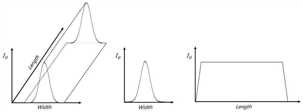
[0113] (a) Implant N-stop. In order to achieve a relatively deep distribution of N-stop, the method of implanting N-type impurities at a small angle (>100kev, tilt 0°) with medium and high energy is usually used to form a near-Gaussian distribution of impurity body concentration along the depth direction. curve, the dotted line indicates the distribution of implanted impurities.

[0114] (b) The laser activates the N-stop, which generally has a lower concentration and a deeper depth, and the depth range is generally 0-10um. The laser emitted by the aforementioned laser annealing system is used to provide a temperature field, so that the required depth is above and the temperature is greater than 1100K, which can satisfy the activation in the full depth range. The solid line indicates the distribution of activated impurities.

[0115] (c) Inject P+ into the collector region. In order to achieve a relatively shallow distribution of P+ in the collector region, a method of implant...

Embodiment 2

[0118] (a) Implant N-stop. In order to achieve a relatively deep distribution of N-stop, the method of implanting (>100kev) N-type impurities is usually used to form a curve of impurity body concentration near Gaussian distribution along the depth direction. The dotted line indicates the implanted impurities Distribution;

[0119] (b) Laser activates N-stop, which generally has a low concentration and deep depth, and the depth range is generally 0-10um. When the laser adjustable space is limited and the temperature field distribution is very steep, it is necessary to use the short-term laser annealing system The wavelength laser performs surface melting, and cooperates with long-wavelength laser to achieve a deeper temperature greater than 1100K, so as to realize activation. The melting depth a is the depth of solid phase to liquid phase transformation, and the solid line indicates the distribution of activated impurities;

[0120] (c) Inject P+ into the collector region. In o...

Embodiment 3

[0123] (a) N-stop implantation. Since the method of implanting N-type impurities with medium and high energy (>100kev) is costly, this embodiment adopts low-energy and high-density implantation of N-type impurities, and the impurities gather on the shallow surface. The dotted line indicates the implantation of impurities Distribution;

[0124] (b) Laser activates N-stop. According to the requirements of device design, the short-wavelength laser of the aforementioned laser annealing system is used to melt the surface of the wafer to the required depth, so as to realize the flat-top distribution of impurity concentration along the depth direction, and the melting depth c For the depth of solid phase to liquid phase transformation, the temperature in this depth range after melting is greater than 1685K in combination with long-wavelength laser, so that the impurities are completely activated, and the solid line indicates the distribution of activated impurities;

[0125] (c) Inje...


PUM

PropertyMeasurementUnit
Thicknessaaaaaaaaaa
Wavelengthaaaaaaaaaa

Abstract

The invention relates to a laser annealing method of a power device, in the annealing process, short-wavelength laser and long-wavelength laser are used for annealing activation, the wavelength rangeof the short-wavelength laser is 300nm to 560nm, and the wavelength range of the long-wavelength laser is 780nm to 1064nm; by selecting laser mixed configurations with different wavelengths for use, ion annealing in different melting ranges and impurity distribution depth ranges and implantation annealing of multiple layers of impurity ions are realized, and meanwhile, the laser mixed configurations with proper wavelengths are selected for use by comprehensively considering the temperature resistance and fragment resistance of different types of wafers; therefore, shallow surface activation under different thermal budget conditions is realized. The invention provides the laser annealing method and a laser annealing system for the power device, which control impurity activation efficiency and impurity distribution by using laser annealing and avoid the technical problem of fragments caused by heat accumulation due to overhigh temperature in the laser annealing process.

Description

technical field [0001] The invention relates to the technical field of laser annealing in the semiconductor industry, in particular to a laser annealing method and a laser annealing system for controlling impurity activation and impurity distribution by using laser annealing. Background technique [0002] In the manufacture of semiconductor chips, ion implantation will be performed on the back of the wafer or the source and drain of some devices. This step will cause serious damage to the crystal lattice, and the doped impurity ions cannot be located in the correct lattice position. , so it does not have effective electrical activity. At this time, the material needs to be heat-treated to repair the lattice damage and activate the electrical activity of impurity ions. This heat treatment process is annealing. [0003] Traditionally used annealing processes, including furnace tube annealing, flash lamp annealing (FLA, Flash Lamp Annealing), spike annealing (Spike Annealing), ...

Claims


Application Information

Patent Timeline
IPC IPC(8): H01L21/268H01L21/324H01L21/331
CPCH01L21/268H01L21/324H01L29/66272
Inventor 蒋一鸣陈静
Owner BEIJING U PRECISION TECH
Why Eureka
Try Eureka