Self-purification silicon wafer transportation device

A transportation device and self-purification technology, applied in transportation and packaging, conveyor objects, electrical components, etc., can solve the problems of reduced silicon wafer performance, silicon wafer damage, etc., to avoid pollution, reasonable structure, and dust isolation.

Pending Publication Date: 2021-03-02
无锡江松科技股份有限公司
View PDF0 Cites 0 Cited by
  • Summary
  • Abstract
  • Description
  • Claims
  • Application Information

AI Technical Summary

Problems solved by technology

[0003] After the silicon wafer is cut, it needs to go through a series of transportation before it can be transported into the reaction chamber for processing reaction. However, the surface of the silicon wafer is often contaminated with dust and other stains during transportation, which will cause damage to the silicon wafer. Reduce the performance of the silicon wafer

Method used


Image

  • Self-purification silicon wafer transportation device
  • Self-purification silicon wafer transportation device
  • Self-purification silicon wafer transportation device

Examples


Embodiment Construction

[0031] The present invention will be further described below in conjunction with the accompanying drawings and specific embodiments, so that those skilled in the art can better understand the present invention and implement it, but the examples given are not intended to limit the present invention.

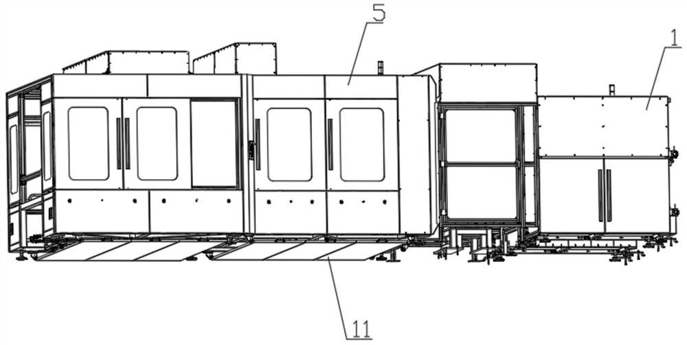
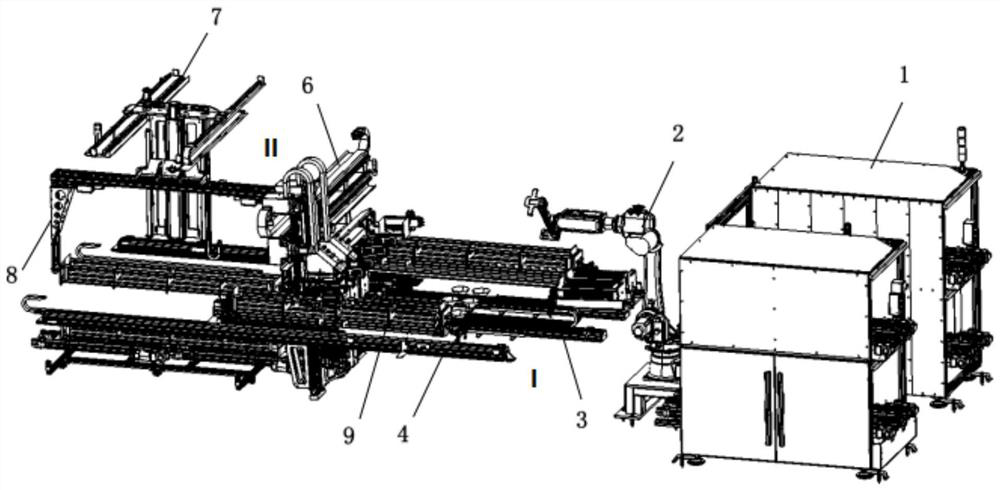
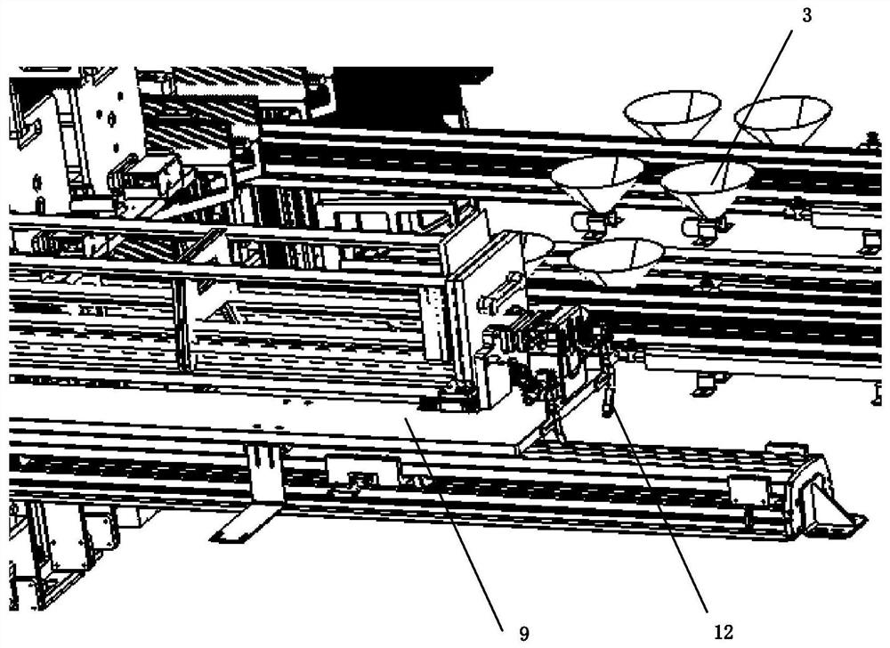
[0032] refer to figure 1 As shown, an embodiment of the present invention includes a symmetrically arranged conveying device 1, a dust-proof frame 5 is arranged on one side of the conveying device 1, and a manipulator is arranged in the middle of the dust-proof frame 5 on one side of the two conveying devices 1. 2. One side of the manipulator 2 is provided with an adsorption and purge runway 3, and both sides of the adsorption and purge runway 3 are provided with a dust-proof runway 4. A grabbing device 6 is arranged above the runway 4, and a truss 7 is arranged on one side of the grabbing device 6 inside the dust-proof frame 5, and a gripper 8 is arranged on the truss 7; On the ...


PUM


Abstract

The invention relates to the technical field of silicon wafer conveying, in particular to a self-purification silicon wafer conveying device. The device comprises conveying devices, and the conveyingdevices are symmetrically arranged; a dustproof rack is arranged on one side of each conveying device, a mechanical arm is arranged at the position, located between one sides of the two conveying devices, in the dustproof rack, an adsorption blowing track is arranged on one side of the mechanical arm, and dustproof runways are arranged on the two sides of the adsorption blowing track; each dustproof runway is arranged on the dustproof rack, a carrying table is arranged on the dustproof runway, a grabbing device is arranged in the dustproof rack and located above the dustproof runway, a truss is arranged in the dustproof rack and located on one side of the grabbing device, and a clamping jaw is arranged on the truss. The device is reasonable and simple in structure and convenient to operate, and therefore outside dust can be isolated in the silicon wafer conveying process, and damage to silicon wafers is avoided.

Description

technical field [0001] The invention relates to the technical field of silicon wafer transportation, in particular to a self-purifying silicon wafer transportation device. Background technique [0002] Cells made of silicon wafers are generally divided into monocrystalline silicon, polycrystalline silicon, and amorphous silicon. Monocrystalline silicon solar cells are currently the fastest developed type of solar cells. Its structure and production process have been finalized, and its products have been widely used in space and on the ground. This solar cell is made of high-purity monocrystalline silicon rods. In order to reduce production costs, solar cells for ground applications use solar-grade monocrystalline silicon rods, and the material performance indicators have been relaxed. Some can also use the head and tail materials and waste single crystal silicon materials processed by semiconductor devices, and make single crystal silicon rods dedicated to solar cells afte...

Claims


Application Information

Patent Timeline
IPC IPC(8): H01L21/677H01L21/67
CPCH01L21/67028H01L21/67733
Inventor 王小彬董晓清
Owner 无锡江松科技股份有限公司
Why Eureka
Try Eureka