Metal contact structure of two-dimensional semiconductor material and preparation method thereof
A two-dimensional semiconductor and metal contact technology, applied in semiconductor/solid-state device manufacturing, semiconductor devices, electrical components, etc., can solve the problems that are not conducive to improving the electrical performance of devices, hindering charge injection and output, and lattice damage of two-dimensional materials, etc. problems, to alleviate the charge congestion effect, improve the switching ratio, and increase the contact area.
- Summary
- Abstract
- Description
- Claims
- Application Information
AI Technical Summary
Problems solved by technology
Method used
Image


Examples
Embodiment Construction
[0027] Embodiments of the present invention are described in detail below, examples of which are shown in the drawings, wherein the same or similar reference numerals designate the same or similar materials or methods having the same or similar functions throughout. The embodiments described below by referring to the figures are exemplary only for explaining the present invention and should not be construed as limiting the present invention. To simplify the disclosure of the present invention, the materials and methods of specific examples are described below. Of course, they are only examples and are not intended to limit the invention. In addition, various specific process and material examples are provided herein, but one of ordinary skill in the art will recognize the applicability of other processes and / or the use of other materials.
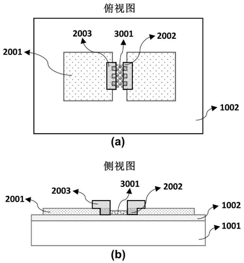
[0028] Hereinafter, an example of a metal contact structure of a two-dimensional semiconductor material and a manufacturing method thereo...
PUM
 Abstract
Description
Claims
Application Information
 - R&D
- Intellectual Property
- Life Sciences
- Materials
- Tech Scout
- Unparalleled Data Quality
- Higher Quality Content
- 60% Fewer Hallucinations
Browse by: Latest US Patents, China's latest patents, Technical Efficacy Thesaurus, Application Domain, Technology Topic, Popular Technical Reports.
© 2025 PatSnap. All rights reserved.Legal|Privacy policy|Modern Slavery Act Transparency Statement|Sitemap|About US| Contact US: help@patsnap.com