Epitaxial wafer of light emitting diode and manufacturing method thereof

A technology of a light-emitting diode and a manufacturing method, applied in the field of optoelectronics, can solve the problems of low light extraction efficiency of deep ultraviolet light-emitting diodes, and achieve the effects of increasing light extraction efficiency, high crystal quality, and reducing total reflection of light.

Active Publication Date: 2022-04-15
HC SEMITEK ZHEJIANG CO LTD
View PDF8 Cites 0 Cited by
  • Summary
  • Abstract
  • Description
  • Claims
  • Application Information

AI Technical Summary

Problems solved by technology

However, the band gap of the p-type GaN material is narrow, and its absorption rate for the deep ultraviolet light band is quite high, which will easily cause the photons of the deep ultraviolet light-emitting diode to be absorbed by the p-type GaN material, making the light extraction efficiency of the deep ultraviolet light-emitting diode very low

Method used


Image

  • Epitaxial wafer of light emitting diode and manufacturing method thereof
  • Epitaxial wafer of light emitting diode and manufacturing method thereof
  • Epitaxial wafer of light emitting diode and manufacturing method thereof

Examples


Embodiment Construction

[0026] In order to make the purpose, technical solution and advantages of the present disclosure clearer, the implementation manners of the present disclosure will be optionally described in detail below in conjunction with the accompanying drawings.

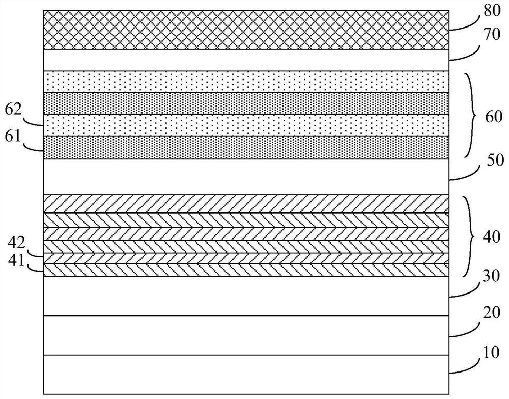
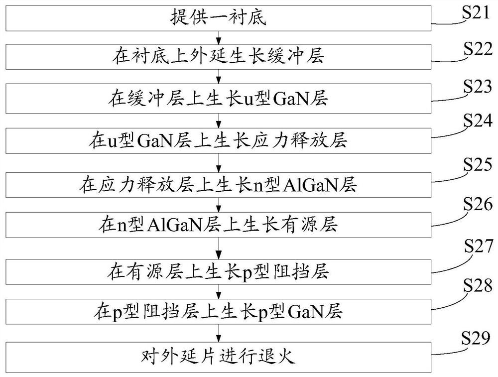
[0027] figure 1 It is a schematic structural diagram of an epitaxial wafer of a light emitting diode provided by an embodiment of the present disclosure. The light emitting diode is an ultraviolet light emitting diode. like figure 1 As shown, the epitaxial wafer includes a substrate 10 and a buffer layer 20 , an n-type AlGaN layer 50 , an active layer 60 , a p-type barrier layer 70 and a p-type GaN layer 80 sequentially stacked on the substrate 10 .

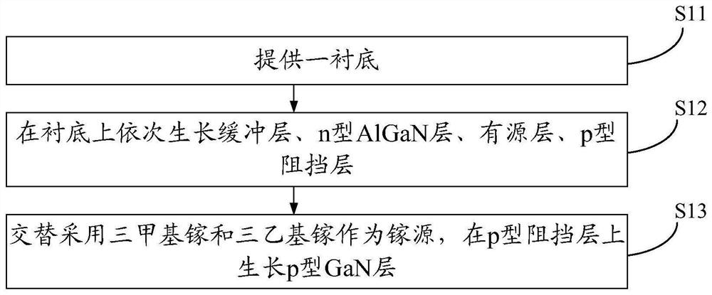
[0028] In the disclosed embodiment, when growing the p-type GaN layer 80 , trimethylgallium and triethylgallium are alternately used as the gallium source.

[0029] By growing the p-type GaN layer on the p-type barrier layer, trimethylgallium and triethylgallium are alternately ...


PUM

PropertyMeasurementUnit
temperatureaaaaaaaaaa
pressureaaaaaaaaaa
thicknessaaaaaaaaaa

Abstract

The disclosure discloses an epitaxial wafer of a light-emitting diode and a manufacturing method thereof, belonging to the field of optoelectronic technology. The manufacturing method includes: providing a substrate; sequentially growing a buffer layer, an n-type AlGaN layer, an active layer, and a p-type barrier layer on the substrate; alternately using trimethylgallium and triethylgallium as a gallium source, and at p A p-type GaN layer is grown on the barrier layer. When trimethylgallium is used as a gallium source for growth, the grown surface has low flatness, which is conducive to roughening the surface, which can reduce the total reflection of light and improve light scattering. When triethylgallium is used as a gallium source for growth, The film formed by growth has high crystal quality, which is beneficial to Mg doping, can increase the concentration of holes, and is beneficial to improving luminous efficiency. By reducing the total reflection of light, increasing the scattering of light and increasing the concentration of holes, the light extraction efficiency of the deep ultraviolet light-emitting diode is increased as a whole.

Description

technical field [0001] The disclosure relates to the field of optoelectronic technology, in particular to an epitaxial wafer of a light emitting diode and a manufacturing method thereof. Background technique [0002] Light Emitting Diode (English: Light Emitting Diode, referred to as: LED), as a very influential new product in the optoelectronics industry, has the characteristics of small size, long service life, colorful colors, and low energy consumption. It is widely used in lighting, display screens , signal lights, backlight, toys and other fields. The core structure of the LED is the epitaxial wafer, and the production of the epitaxial wafer has a great influence on the photoelectric characteristics of the LED. [0003] An epitaxial wafer generally includes a buffer layer, an n-type layer, an active layer, a p-type barrier layer, and a p-type layer. [0004] P-type AlGaN is more suitable as the material for making the p-type layer of deep ultraviolet light-emitting d...

Claims


Application Information

Patent Timeline
Patent Type & Authority Patents(China)
IPC IPC(8): H01L33/00H01L33/04H01L33/12H01L33/22
CPCH01L33/007H01L33/04H01L33/12H01L33/22
Inventor 丁涛龚程成尹涌梅劲
Owner HC SEMITEK ZHEJIANG CO LTD
Why Eureka
Try Eureka