Epitaxial wafer of gallium nitride-based light-emitting diode and preparation method thereof

A light-emitting diode, gallium nitride-based technology, applied in semiconductor devices, electrical components, circuits, etc., can solve the problems of low luminous efficiency of light-emitting diodes, achieve the effects of improving energy band difference, improving luminous efficiency, and improving crystal quality

Active Publication Date: 2019-06-28
HC SEMITEK ZHEJIANG CO LTD
View PDF3 Cites 0 Cited by
  • Summary
  • Abstract
  • Description
  • Claims
  • Application Information

AI Technical Summary

Problems solved by technology

[0006] In order to solve the problem in the prior art that the pedestal absorbs light emitted to the sapphire substrate, resulting in low luminous efficiency of the light-emitting diode, an embodiment of the present invention provides an epitaxial wafer of a gallium nitride-based light-emitting diode and a preparation method thereof

Method used


Image

  • Epitaxial wafer of gallium nitride-based light-emitting diode and preparation method thereof
  • Epitaxial wafer of gallium nitride-based light-emitting diode and preparation method thereof

Examples


Embodiment 1

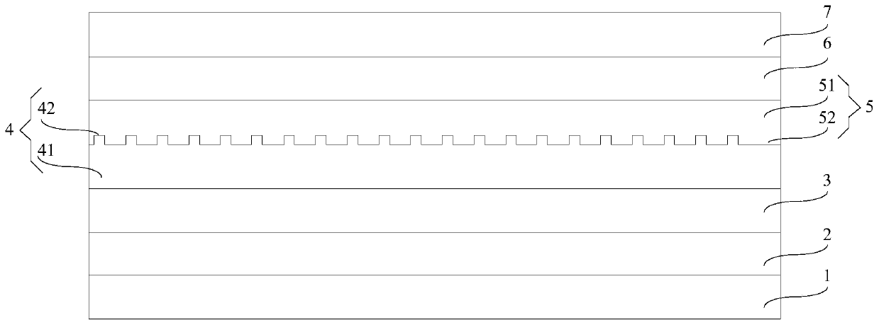
[0037] An embodiment of the present invention provides an epitaxial wafer of a gallium nitride-based light-emitting diode, see figure 1 , the epitaxial wafer includes a sapphire substrate 1, and a gallium nitride buffer layer 2, an undoped gallium nitride layer 3, an N-type gallium nitride layer 4, a multi-quantum well layer 5, P-type AlGaN layer 6 and P-type GaN layer 7 .

[0038] In this embodiment, the N-type GaN layer 4 includes an N-type GaN layer body 41 and a plurality of protrusions 42, the N-type GaN layer body 41 is a columnar structure, and the N-type GaN layer body 41 The bottom surface of the N-type GaN layer body 41 is disposed on the undoped GaN layer 3 , and a plurality of protrusions 42 are arranged in an array on the top surface of the N-type GaN layer body 41 . The multi-quantum well layer 5 includes a multi-quantum well layer body 51 and a filling part 52, and the filling part 52 is arranged on the N-type gallium nitride layer body 41 exposed between the p...

Embodiment 2

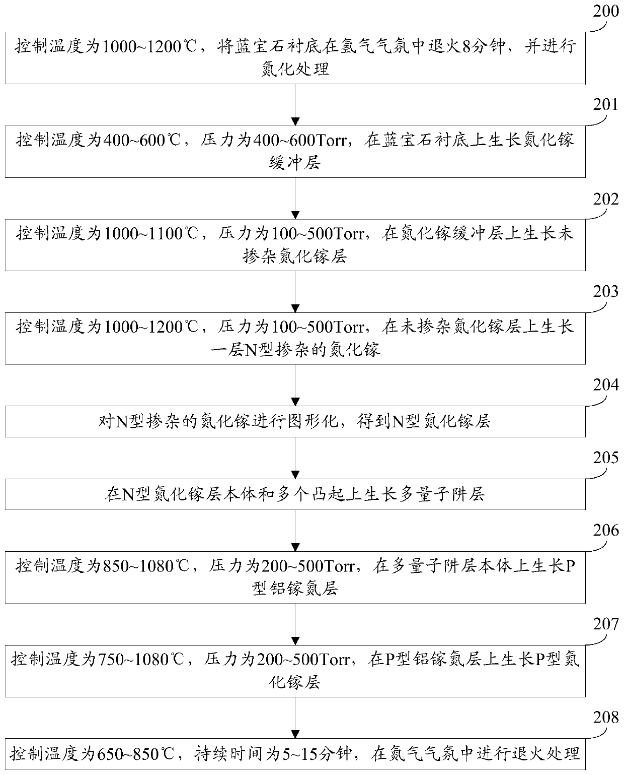
[0061] An embodiment of the present invention provides a method for preparing an epitaxial wafer of a gallium nitride-based light-emitting diode, which is suitable for preparing the epitaxial wafer provided in Embodiment 1. See figure 2 , the preparation method comprises:

[0062] Step 200: Control the temperature to 1000-1200° C., anneal the sapphire substrate in a hydrogen atmosphere for 8 minutes, and perform nitriding treatment.

[0063] Understandably, step 200 may serve to clean the surface of the sapphire substrate.

[0064] In this embodiment, controlling the temperature and pressure both refers to controlling the temperature and pressure in the reaction chamber for growing epitaxial wafers, which will not be described in detail below.

[0065] In this embodiment, the sapphire substrate adopts [0001] crystal orientation sapphire.

[0066] Step 201: Control the temperature to 400-600° C. and the pressure to 400-600 Torr to grow a GaN buffer layer on the sapphire subs...


PUM

PropertyMeasurementUnit
heightaaaaaaaaaa
heightaaaaaaaaaa
thicknessaaaaaaaaaa

Abstract

The invention discloses an epitaxial wafer of a gallium nitride based light emitting diode and a preparation method thereof, which belongs to the technical field of semiconductors. The epitaxial wafer comprises a sapphire substrate, a gallium nitride buffer layer, an undoped gallium nitride layer, an N-type gallium nitride layer, a multi-quantum well layer, a P-type aluminum gallium nitride layer and a P-type gallium nitride layer. The N-type gallium nitride layer comprises an N-type gallium nitride layer body and a number of protrusions. The N-type gallium nitride layer body is in a column structure. The bottom of the N-type gallium nitride layer body is arranged on the undoped gallium nitride layer. A number of protrusions are arranged on the top of the N-type gallium nitride layer body in array. The multi-quantum well layer comprises a multi-quantum well layer body and a filling part. The filling part is arranged on the N-type gallium nitride layer body exposed among a number of protrusions and fills spaces among a number of protrusions. The filling part and a number of protrusions form a column structure. The multi-quantum well layer body is a column structure. The multi-quantum well layer body is arranged on the column structure composed of the filling part and a number of protrusions. The epitaxial wafer provided by the invention has the advantage of high luminous efficiency.

Description

technical field [0001] The invention relates to the technical field of semiconductors, in particular to an epitaxial wafer of a gallium nitride-based light-emitting diode and a preparation method thereof. Background technique [0002] Light Emitting Diode (English: Light Emitting Diode, referred to as: LED) is a semiconductor device that can effectively convert electrical energy into light energy. Currently, LEDs include gallium nitride-based LEDs and aluminum gallium indium phosphorus-based LEDs, of which gallium nitride-based LEDs received more and more attention and research. [0003] The epitaxial wafer of gallium nitride-based LED includes a sapphire substrate, and a gallium nitride buffer layer, an undoped gallium nitride layer, an n-type gallium nitride layer, and a multi-quantum well layer (English: Multiple Quantum Well, referred to as: MQW), P-type aluminum gallium nitride layer and P-type gallium nitride layer. When a current passes through the GaN-based LED, el...

Claims


Application Information

Patent Timeline
Patent Type & Authority Patents(China)
IPC IPC(8): H01L33/00H01L33/06H01L33/22H01L33/32H01L33/58H01L33/60
CPCH01L33/0054H01L33/06H01L33/22H01L33/325H01L33/58H01L33/60H01L2933/0008H01L2933/0033H01L2933/0058
Inventor 王群郭炳磊董彬忠李鹏王江波
Owner HC SEMITEK ZHEJIANG CO LTD
Why Eureka
Try Eureka