A long-wave infrared broadband achromatic metasurface lens

A long-wave infrared and metasurface technology, applied in the field of infrared imaging and micro-nano photonics, can solve the problem of inability to eliminate broadband light chromatic aberration, achieve smooth structural changes, suppress scattering effects, and ensure achromatic effects

Active Publication Date: 2021-10-08
HUAZHONG UNIV OF SCI & TECH
View PDF2 Cites 0 Cited by
  • Summary
  • Abstract
  • Description
  • Claims
  • Application Information

AI Technical Summary

Problems solved by technology

[0007] Aiming at the defects and improvement needs of the prior art, the present invention provides a long-wave infrared broadband achromatic metasurface lens, the purpose of which is to solve the technical problem that the existing metasurface lens cannot eliminate the chromatic aberration of broadband light in the long-wave infrared band

Method used


Image

  • A long-wave infrared broadband achromatic metasurface lens
  • A long-wave infrared broadband achromatic metasurface lens
  • A long-wave infrared broadband achromatic metasurface lens

Examples


Embodiment 1

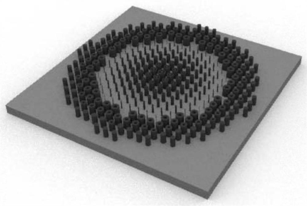
[0078] A long-wave infrared broadband achromatic metasurface lens with a diameter of 240 μm and a numerical aperture of 0.5 can achieve high-efficiency achromatic near-diffraction-limited focusing at any wavelength within the working wavelength range of 8-12 μm. In this embodiment, the average back focal length of the lens is 208 μm, and the maximum axial focal length drift is less than 4%. The three-dimensional schematic diagram of the metalens is as follows figure 1 As shown, the schematic diagram of the two-dimensional structure on the vertical section of the metalens is as follows figure 2 shown.

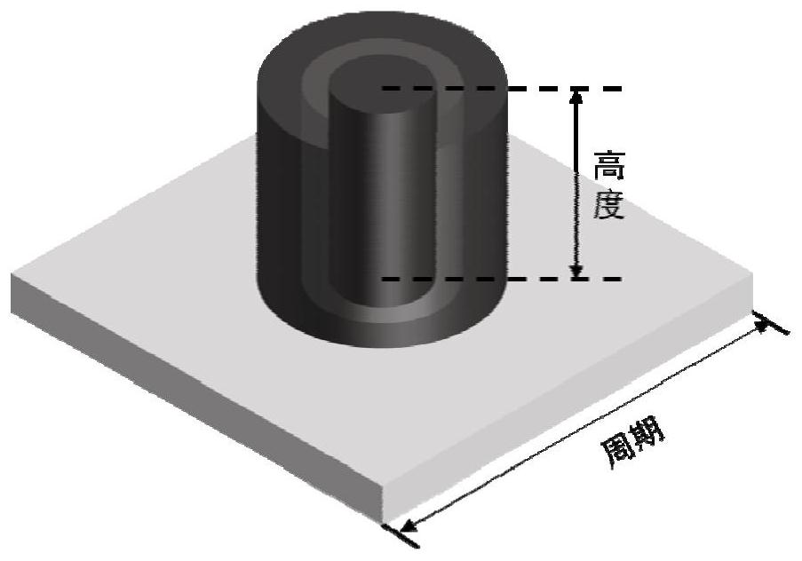
[0079] In this embodiment, in this embodiment, the structure of one of the metasurface lens units is as follows image 3 As shown, the microstructure is a silicon column made of silicon material, and the projection pattern of the microstructure on the dielectric substrate is as follows Figure 4 Among the concentric circular rings shown in (c) are nested circular patterns; in...

Embodiment 2

[0086] A long-wave infrared broadband achromatic metasurface lens with a diameter of 1 mm and a numerical aperture of 0.15. In this embodiment, both the substrate and the microstructure array of the superlens are made of silicon, and the manufacturing process of the superlens is simplified through the all-silicon design, and the manufacturing cycle and cost of the superlens are shortened. In terms of design, the high transmittance window of the metalens unit under the all-silicon material is obtained by scanning the units with different unit period and silicon column height parameter combinations, and the unit period is 3.5 μm, and the height is 8 μm. The high transmittance size combination is selected. According to the phase and dispersion formula under the parameters of diameter 1mm and numerical aperture 0.15, the theoretical distribution of phase-dispersion on the surface of the metalens is obtained.

[0087] For the simulation and optimization methods of the phase-dispers...


PUM

PropertyMeasurementUnit
heightaaaaaaaaaa
heightaaaaaaaaaa
heightaaaaaaaaaa

Abstract

The invention discloses a long-wave infrared broadband achromatic metasurface lens, which belongs to the field of infrared imaging and micro-nano photonics. The metasurface lens units in the metasurface lens are periodically arranged in the form of a square lattice; the metasurface lens units It is composed of a dielectric substrate and a microstructure located in the center of the dielectric substrate, and the projection pattern of the microstructure on the dielectric substrate is a figure that is rotationally symmetrical about a 90° angle; the phase and phase dispersion introduced by the microstructure at different positions satisfy and The microstructure selection method at each position is as follows: according to the above two formulas, the theoretical parameter combination is obtained, and the phase of the unit where each microstructure is located and the corresponding phase dispersion are obtained through weighted first-order linear fitting, which is recorded as the actual parameter combination. Each parameter combination is drawn in the same scatter diagram, and the microstructure corresponding to the actual parameter combination closest to the theoretical parameter combination is selected. The invention can realize broadband achromatic aberration in the long-wave infrared band.

Description

technical field [0001] The invention belongs to the fields of infrared imaging and micro-nano photonics, and more specifically relates to a long-wave infrared broadband achromatic metasurface lens. Background technique [0002] In traditional infrared optical systems, refractive optical elements such as glass lenses are usually used to achieve imaging. This type of lens realizes the regulation of light through the refraction of the front and rear surfaces. Compared with the overall volume of the lens, the actual working area volume is low in space utilization, resulting in The problem of miniaturization and miniaturization of the optical system is solved. As an emerging sub-wavelength artificial material, metasurfaces can be arbitrarily adjusted to various optical properties such as the amplitude and phase of the incident light through the artificial design of the array unit, resulting in a series of novel physical properties, such as negative refraction. High-efficiency ma...

Claims


Application Information

Patent Timeline
Patent Type & Authority Patents(China)
IPC IPC(8): G02B3/00G02B1/00
CPCG02B1/002G02B3/0037
Inventor 易飞邬灏侯铭铭
Owner HUAZHONG UNIV OF SCI & TECH
Why Eureka
Try Eureka