Method and device for grading and screening chips and electronic equipment

A grading and chip technology, applied in the grading field, can solve the problems of inconvenient packaging operation, no difference in the quality of wafers and wafers, inaccurate classification results, etc., to achieve high yield and reliability, and improve product quality. rate, good efficiency and the effect of the market

Active Publication Date: 2021-04-02
HYGON INFORMATION TECH CO LTD
View PDF8 Cites 9 Cited by
  • Summary
  • Abstract
  • Description
  • Claims
  • Application Information

AI Technical Summary

Problems solved by technology

[0003] The classification and distinction of chips by SBO only considers the parameter distribution of WS, and does not consider the key process characteristic characterization data (WAT Data, wafer electrical parameter data), and at the same time does not involve the quality difference between wafers and wafers , so that chips with qualified indicators are often selected for use in products on wafers with poor performance and quality. In fact, such chips do not meet the classification specifications of high-quality products.
[0004] At present, the American Sandisk company uses the quality grade classification of wafers and chips when producing Flash memory products. It makes full use of the WS test data of Memory products and finely distinguishes wafers and chips, but still does not introduce the WAT key process. characteristic data
At the same time, there is also a lack of chip classification sources in the assembly map, which is not convenient for subsequent packaging operations, the classification results are not accurate enough, and product yield control is not good

Method used


Image

  • Method and device for grading and screening chips and electronic equipment
  • Method and device for grading and screening chips and electronic equipment
  • Method and device for grading and screening chips and electronic equipment

Examples


Embodiment Construction

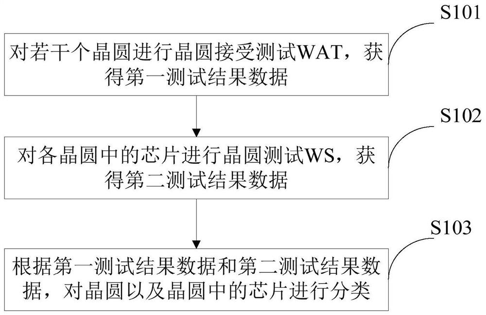
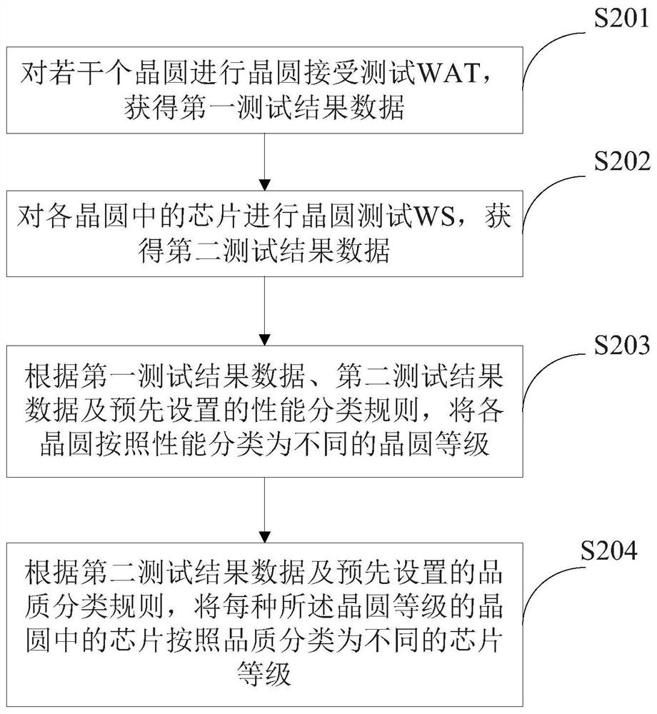
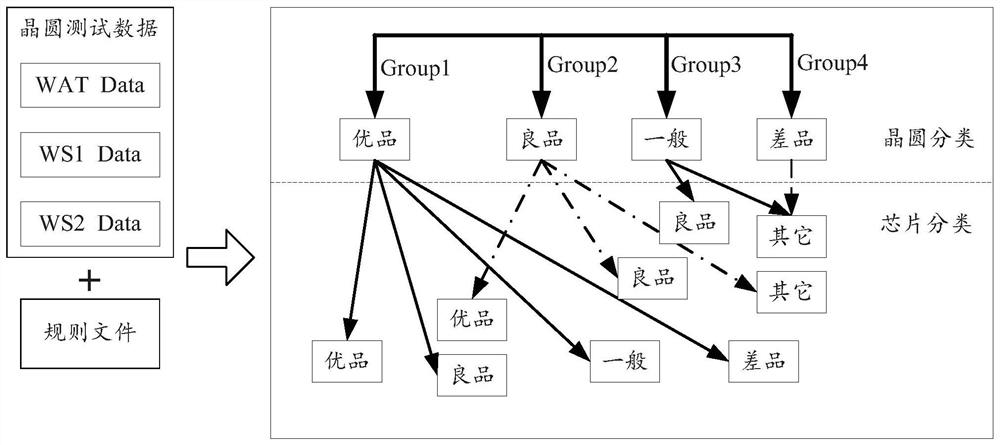
[0044] The present invention considers that there are quality differences between wafers in the same batch of wafer production, and it is necessary to classify the quality of wafers as high, medium, and low grades; at the same time, there are also chip performance differences in the wafers, which are used in wafer packaging and packaging. Before plastic packaging, the script can be used to classify the quality according to the key index parameter specifications, and generate the packaging coordinates of the three-dimensional array, mark the chip level, and use it for different grades of products after plastic packaging. Embodiments of the present invention will be described in detail below in conjunction with the accompanying drawings.

[0045]It should be clear that the described embodiments are only some of the embodiments of the present invention, not all of them. Based on the embodiments of the present invention, all other embodiments obtained by persons of ordinary skill ...


PUM


Abstract

The embodiment of the invention discloses a method and device for grading and screening chips and electronic equipment, relates to the technical field of chip grading, and solves the problem that selected chips cannot meet the requirements of high-quality products due to the fact that the chips with qualified indexes are selected from wafers with poor performance and quality to be used by the products. The method for grading and screening the chips comprises the following steps: carrying out wafer acceptance testing (WAT) on a plurality of wafers to obtain first test result data; carrying outwafer testing WS on the chips in the wafers to obtain second testing result data; and classifying the wafers and the chips in the wafers according to the first testing result data and the second testing result data. According to the method, the wafers of different quality grades can be split according to the WAT and WS testing result data, and chips of different qualities can be classified for useby products of different grades during subsequent sealing testing.

Description

technical field [0001] The invention relates to the technical field of chip grading, in particular to a method, device and electronic equipment for grading and screening chips. Background technique [0002] In the existing chip testing process, after the chip completes the wafer-level sorting test WS (Wafer sorting) test, the chip discards the die that failed the Binning test, and then picks the pass die for packaging. For Pass die , first test Bin classification optimization SBO (sort bin optimizer), and then package the die classified into different product categories, so as to perform final test FT (Final Test) on products of different quality, and finally conduct system-level testing and deliver to customers . For chip bin classification optimization, refer to the 4 WS key parameter values. The parameter specifications of different levels of chips are determined by the parameter distribution ratio, product specification requirements, and packaging and testing type requi...

Claims


Application Information

Patent Timeline
Patent Type & Authority Applications(China)
IPC IPC(8): B07C5/344B07C5/36G06K9/62
CPCB07C5/344B07C5/361B07C5/362G06F18/24
Inventor 文波
Owner HYGON INFORMATION TECH CO LTD
Why Eureka
Try Eureka