Supercharge Your Innovation With Domain-Expert AI Agents!

Multi-chip package and manufacturing method thereof

A multi-chip packaging and chip technology, used in semiconductor/solid-state device manufacturing, electrical components, semiconductor devices, etc., can solve problems such as limited signal communication speed, and achieve the effect of improving overall performance

Pending Publication Date: 2021-04-13
IND TECH RES INST
View PDF0 Cites 1 Cited by
  • Summary
  • Abstract
  • Description
  • Claims
  • Application Information

AI Technical Summary

Problems solved by technology

However, the signal communication speed between multiple semiconductor chips in the existing multi-chip package is limited, so the overall performance of the semiconductor package still needs to be further improved

Method used


Image

  • Multi-chip package and manufacturing method thereof
  • Multi-chip package and manufacturing method thereof
  • Multi-chip package and manufacturing method thereof

Examples


Embodiment Construction

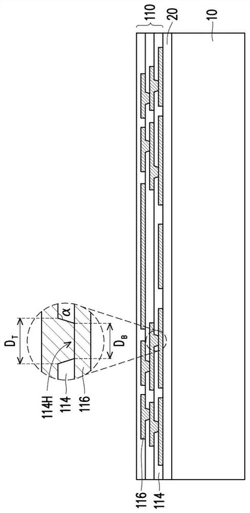
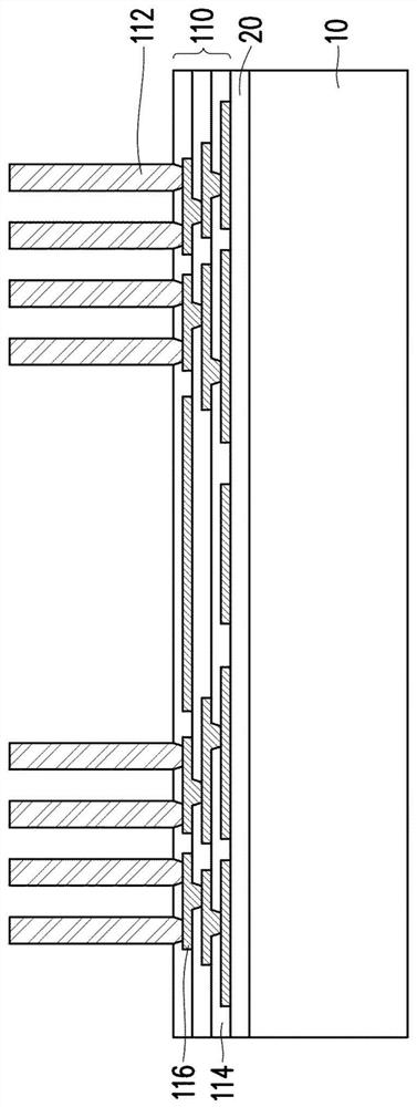
[0127] Reference will now be made in detail to the exemplary embodiments of the present invention, examples of which are illustrated in the accompanying drawings. Wherever possible, the same reference numbers will be used in the drawings and description to refer to the same or like parts.

[0128] The following examples are listed and described in detail with the accompanying drawings, but the provided examples are not intended to limit the scope of the present invention. In addition, the drawings are for illustration purposes only and are not drawn according to the original scale, and different film layers or regions may be enlarged or reduced to be shown in a single drawing. Also, although terms such as "first", "second", etc. are used herein to describe various elements, regions and / or components, these elements, regions and / or components should not be limited by these terms. Rather, these terms are only used to distinguish one element, region or component from another ele...


PUM

PropertyMeasurementUnit
Melting pointaaaaaaaaaa

Abstract

The invention discloses a multi-chip package and a manufacturing method thereof. The multi-chip package includes a redistribution circuit structure; a first semiconductor chip disposed on the redistribution structure and having a first active surface on which a first conductive post is disposed; a second semiconductor chip disposed above the first semiconductor chip and having a second active surface on which a first conductor is disposed; and a first encapsulant disposed on the redistribution circuit structure and encapsulating at least the first semiconductor chip, wherein the first conductive post and the first conductor are aligned and bonded to each other to electrically connect the first semiconductor chip and the second semiconductor chip.

Description

technical field [0001] The present invention relates to a semiconductor package and a manufacturing method thereof, and in particular to a multi-chip package and a manufacturing method thereof. Background technique [0002] In order to make the semiconductor package have both thin and light volume and high performance, the current packaging technology has tried to integrate multiple semiconductor chips into a single semiconductor package to form a multi-chip package or stack multiple semiconductor packages with 3D stacking technology. A stacked package (Package on package, PoP) structure is formed. However, the signal communication speed between multiple semiconductor chips in the existing multi-chip package is limited, so the overall performance of the semiconductor package still needs to be further improved. Contents of the invention [0003] The object of the present invention is to provide a multi-chip package with good performance. [0004] The invention provides a ...

Claims


Application Information

Patent Timeline
IPC IPC(8): H01L23/498H01L23/538H01L27/146H01L21/48H01L21/768
CPCH01L27/14636H01L27/14634H01L27/1469H01L23/49838H01L23/5386H01L21/4846H01L21/76895H01L2224/92244H01L2224/32225H01L2224/04105H01L2224/12105H01L2224/16235H01L2224/73204H01L2224/81005H01L2224/16227H01L2224/73267H01L2224/16145H01L2224/32145H01L2924/18162H01L2924/15311H01L2924/15321H01L2224/83005H01L2224/73265H01L2224/48227H01L2924/15331H01L2924/00H01L2224/16225
Inventor 林育民林昂樱吴昇财陈昭蓉倪梓瑄黄馨仪罗元听
Owner IND TECH RES INST
Features
  • R&D
  • Intellectual Property
  • Life Sciences
  • Materials
  • Tech Scout
  • Unparalleled Data Quality
  • Higher Quality Content
  • 60% Fewer Hallucinations
Learn More