

Using stochastic failure metrics in semiconductor manufacturing
一种随机故障、半导体的技术,应用在半导体/固态器件制造、半导体/固态器件测试/测量、测量装置等方向,能够解决无法适时方式涵盖关键特征、未考虑设计等问题
- Summary
- Abstract
- Description
- Claims
- Application Information
AI Technical Summary
Problems solved by technology
Method used
Image

Examples
Embodiment Construction
[0036] While claimed subject matter will be described in terms of particular embodiments, other embodiments, including embodiments that do not provide all of the benefits and features set forth herein, are also within the scope of the disclosure. Various structural, logical, process step and electrical changes may be made without departing from the scope of the present invention. Accordingly, the scope of the invention is defined only by reference to the appended claims.
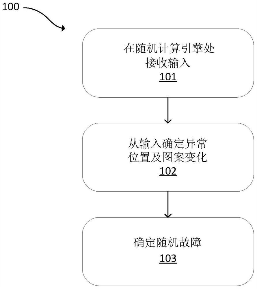
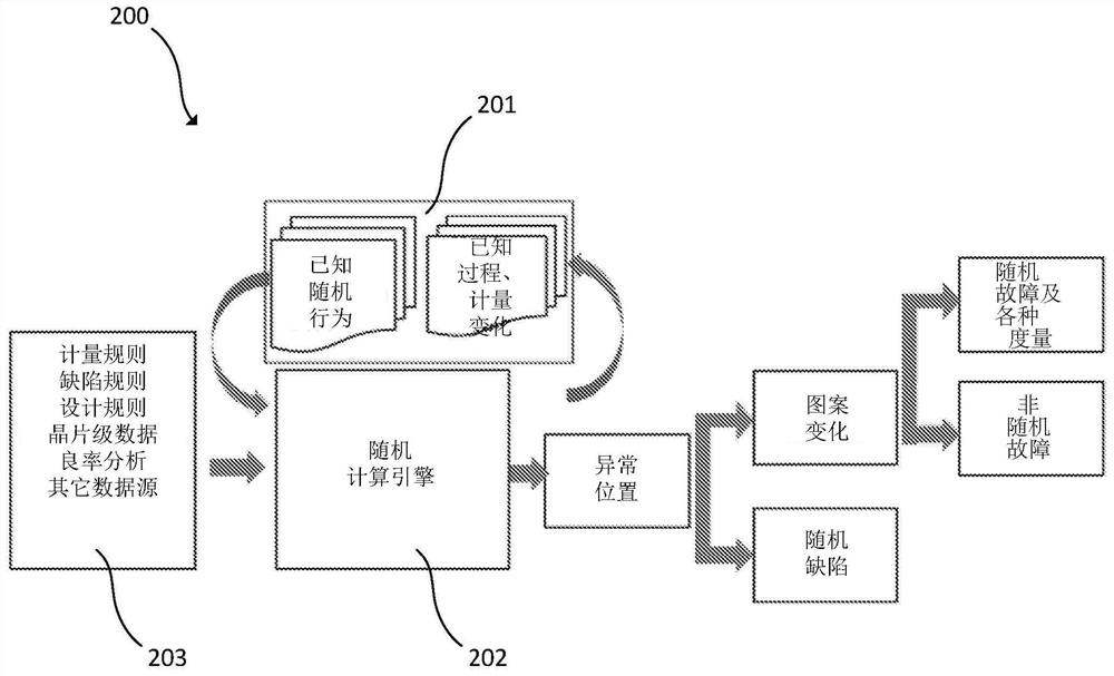
[0037] Embodiments disclosed herein use integrated circuit (IC) design files to guide verification. IC design files can be used for analysis to perform optical and / or e-beam inspection to output random failure metrics of the semiconductor manufacturing process. IC design files can also be used to provide direct output from inspection systems or yield management software.
[0038]In order to obtain a reasonable random failure rate for a given feature with statistical significance, a large area test is usual...
PUM
 Abstract
Description
Claims
Application Information