Supercharge Your Innovation With Domain-Expert AI Agents!

Semiconductor wafer cleaning device and method based on heating and drying mechanism

A technology for heating, drying and cleaning devices, which is used in cleaning methods using liquids, heating to dry solid materials, drying solid materials, etc., to improve cleaning efficiency, avoid tilting, and avoid excessive deposition of water droplets.

Active Publication Date: 2021-04-30
JIANGSU ASIA ELECTRONICS TECH CO LTD
View PDF6 Cites 0 Cited by
  • Summary
  • Abstract
  • Description
  • Claims
  • Application Information

AI Technical Summary

Problems solved by technology

[0003] The object of the present invention is to provide a semiconductor wafer cleaning device and cleaning method based on a heating and drying mechanism, so as to solve the above-mentioned problem that only a single wafer can be cleaned

Method used


Image

  • Semiconductor wafer cleaning device and method based on heating and drying mechanism
  • Semiconductor wafer cleaning device and method based on heating and drying mechanism
  • Semiconductor wafer cleaning device and method based on heating and drying mechanism

Examples


Embodiment 1

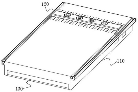
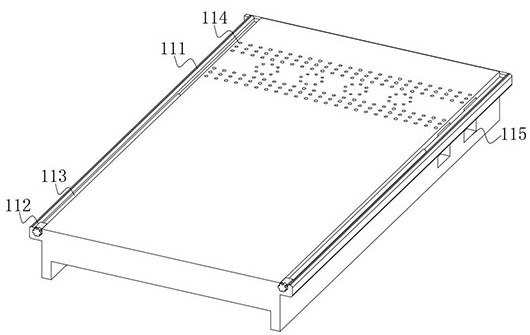
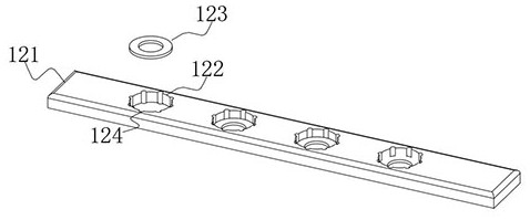
[0066] see Figure 1-12 As shown, one of the purposes of this embodiment is to provide a semiconductor wafer cleaning device based on a heating and drying mechanism, including a bottom mechanism 10, a top mechanism 20 installed on the top of the bottom mechanism 10, and a drying device installed on the side of the top mechanism 20 30. The bottom mechanism 10 includes a bottom plate 110, top grooves 111 are provided on both sides of the top of the bottom plate 110, a placement piece 120 is installed on the top of the bottom plate 110, the placement piece 120 includes a placement plate 121, and several card slots 122 are arranged on the top of the placement plate 121. The bottom end of the groove 122 is provided with a bottom ring 123, and the top mechanism 20 at least includes:

[0067] The support plate 210, the bottom end of the support plate 210 is provided with several hydraulic rods 211, the top of the support plate 210 is provided with a bracket 212, the support 212 is a ...


PUM


Abstract

The invention relates to the technical field of semiconductor wafers, in particular to a semiconductor wafer cleaning device and method based on a heating and drying mechanism. The device comprises a bottom mechanism, a top mechanism installed at the top end of the bottom mechanism and a drying device installed on the side face of the top mechanism. A containing piece is arranged at the top end of the bottom mechanism, a plurality of clamping grooves are formed in the top end of the containing piece, the top mechanism comprises a supporting plate, and a support is arranged at the top end of the supporting plate. A sliding groove is formed in the top end of the support, a cleaning device is arranged in the sliding groove, and the cleaning device is connected with the support in a sliding manner. According to the present invention, through the arrangement of the support and the placement piece, when semiconductor wafers are cleaned, the multiple semiconductor wafers are placed in different clamping grooves, and the cleaning device is slid, so that the multiple semiconductor wafers can be cleaned, and the cleaning efficiency is improved.

Description

technical field [0001] The invention relates to the technical field of semiconductor wafers, in particular to a semiconductor wafer cleaning device and cleaning method based on a heating and drying mechanism. Background technique [0002] Wafer refers to the silicon wafer used to make silicon semiconductor circuits, and its raw material is silicon. High-purity polycrystalline silicon is dissolved and mixed with silicon crystal seeds, and then slowly pulled out to form cylindrical single crystal silicon. After the silicon ingot is ground, polished, and sliced, it forms a silicon wafer, that is, a wafer. At present, the domestic wafer production line is mainly 8 inches and 12 inches. After the semiconductor wafer is finished, it needs to be cleaned in order to remove the stains left on the surface of the wafer during the processing process. Most of the existing cleaning devices for semiconductor wafers can only clean a single wafer, resulting in too slow cleaning efficiency ...

Claims


Application Information

Patent Timeline
Patent Type & Authority Applications(China)
IPC IPC(8): H01L21/67B08B3/02B08B13/00F26B3/28
CPCB08B3/02B08B13/00F26B3/28H01L21/67023H01L21/67034H01L21/67051
Inventor 钱诚李刚童建
Owner JIANGSU ASIA ELECTRONICS TECH CO LTD
Features
  • R&D
  • Intellectual Property
  • Life Sciences
  • Materials
  • Tech Scout
  • Unparalleled Data Quality
  • Higher Quality Content
  • 60% Fewer Hallucinations
Learn More