Semiconductor wafer cleaning device and cleaning method based on heating and drying mechanism
A technology for heating, drying and cleaning devices, which is applied in the direction of using liquid cleaning methods, heating to dry solid materials, and drying solid materials, etc.
- Summary
- Abstract
- Description
- Claims
- Application Information
AI Technical Summary
Problems solved by technology
Method used
Image

Examples
Embodiment 1
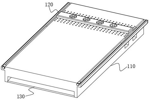
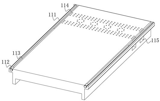
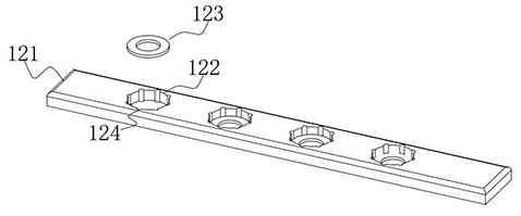
[0066] see Figure 1-12 As shown, one of the purposes of this embodiment is to provide a semiconductor wafer cleaning device based on a heating and drying mechanism, including a bottom mechanism 10, a top mechanism 20 installed on the top of the bottom mechanism 10, and a drying device installed on the side of the top mechanism 20 30. The bottom mechanism 10 includes a bottom plate 110, top grooves 111 are provided on both sides of the top of the bottom plate 110, a placement piece 120 is installed on the top of the bottom plate 110, the placement piece 120 includes a placement plate 121, and several card slots 122 are arranged on the top of the placement plate 121. The bottom end of the groove 122 is provided with a bottom ring 123, and the top mechanism 20 at least includes:
[0067] The support plate 210, the bottom end of the support plate 210 is provided with several hydraulic rods 211, the top of the support plate 210 is provided with a bracket 212, the support 212 is a ...
PUM
 Abstract
Description
Claims
Application Information
 - R&D
- Intellectual Property
- Life Sciences
- Materials
- Tech Scout
- Unparalleled Data Quality
- Higher Quality Content
- 60% Fewer Hallucinations
Browse by: Latest US Patents, China's latest patents, Technical Efficacy Thesaurus, Application Domain, Technology Topic, Popular Technical Reports.
© 2025 PatSnap. All rights reserved.Legal|Privacy policy|Modern Slavery Act Transparency Statement|Sitemap|About US| Contact US: help@patsnap.com