EBCMOS resolution parameter measuring device

A measurement device and resolution technology, applied in the direction of testing optical performance, etc., can solve the problems of noise difference resolution, resolution effect, and can only reflect room temperature conditions, etc., achieve ingenious structure design, improve test efficiency, and solve the problem of water vapor The effect of condensation

Pending Publication Date: 2021-05-07
SONGSHAN LAKE MATERIALS LAB +1
View PDF14 Cites 2 Cited by
  • Summary
  • Abstract
  • Description
  • Claims
  • Application Information

AI Technical Summary

Problems solved by technology

At present, relevant reports and patents have been reported and patented on the measuring device and method of ICCD resolution, such as the publication number "CN105973570B", titled "Low-light ICCD resolution measuring device and measurement method"; ICCD Signal-to-Noise Ratio Test System and Test Method”; however, there is no relevant report on the measuring device for EBCMOS. Results reflect performance at room temperature only
But in fact, the demand for low-light imaging devices is to work outdoors all-weather, and there are extreme operating temperature scenarios. For low-light night visi

Method used


Image

  • EBCMOS resolution parameter measuring device
  • EBCMOS resolution parameter measuring device
  • EBCMOS resolution parameter measuring device

Examples


Embodiment

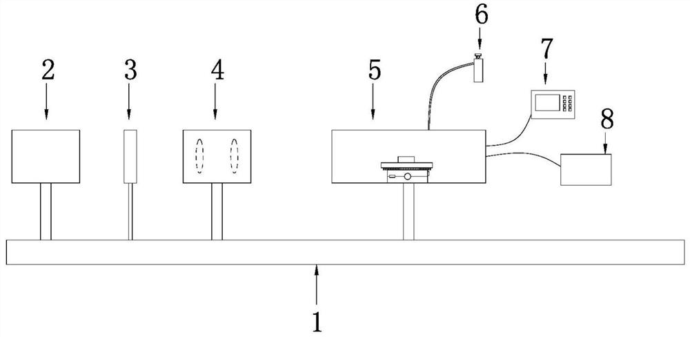
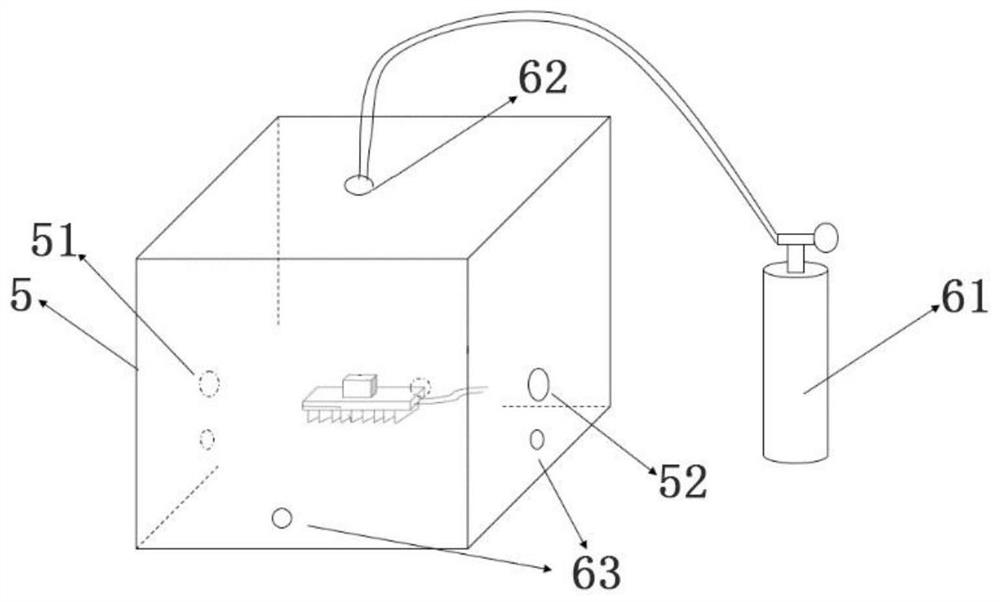
[0020] Example: see figure 1 , figure 2 with image 3 , an EBCMOS resolution parameter measurement device provided by an embodiment of the present invention, which includes an optical platform 1, a light source system 2, a resolution target 3, an objective lens 4, a measurement dark box 5, a gas replacement device 6, a TEC temperature control system 7 and Image acquisition and analysis system8.

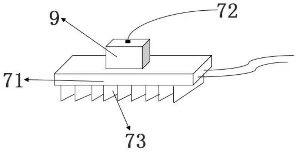
[0021] The light source system 2, resolution target 3, objective lens 4 and measurement dark box 5 are sequentially arranged on the optical platform 1, and the light source system 2 produces an illumination range of 1×10 -6 lx~1x10 2 lx and non-uniformity ≤ 1% outgoing light; the TEC temperature control system 7 includes a TEC temperature control platform 71, a temperature sensor 72 and a temperature control panel, the TEC temperature control platform 71 is arranged in the measurement dark box 5, the The temperature sensor 72 is located on the EBCMOS device 9 on the TEC temperatu...


PUM

PropertyMeasurementUnit
Clear apertureaaaaaaaaaa
Focal lengthaaaaaaaaaa

Abstract

The invention discloses an EBCMOS resolution parameter measuring device. The device comprises an optical platform, a light source system, a resolution target, an objective lens, a measurement camera obscura, a gas replacement device, a TEC temperature control system and an image acquisition and analysis system. The device is ingenious and reasonable in structural design; the illuminance of a light source and the working temperature of a tested device can be changed; a TEC temperature control table is used for independently and only controlling the temperature of the tested device to achieve rapid temperature changing, so that the testing efficiency is improved; the gas replacement device is arranged, so that air in the measurement camera obscura can be rapidly exhausted, and therefore the water vapor content is reduced, the problem that a testing result is affected by potential water vapor condensation and frosting under the cooling condition is effectively solved; and thus, accurate and integrity evaluation testing on the resolution of an EBCMOS device is achieved, the real level of the resolution of the EBCMOS device in the full working temperature range is accurately reflected, it is guaranteed that the device works reliably in various application scenes, and research, development and production work can be guided.

Description

technical field [0001] The invention relates to the technical field of measuring EBCMOS resolution parameters, in particular to a measuring device for EBCMOS resolution parameters. Background technique [0002] Low-light imaging technology is a high-tech research on physical processes such as mutual conversion, enhancement, processing, and display of photo-electronic image information and its realization methods under night sky light or poor visibility conditions. It is the core of modern optoelectronic imaging technology An important component, it has played a huge role in military, public security, astronomy, aerospace, navigation, biology, medicine, nuclear physics, satellite monitoring, high-speed photography and other fields. The core device used in low-light night vision equipment is the various generations of photoelectric imaging devices micro-optical devices. [0003] Electron bombardment-type devices EBCMOS, ICCD, and ICMOS are all digital low-light imaging device...

Claims


Application Information

Patent Timeline
IPC IPC(8): G01M11/02
CPCG01M11/02
Inventor 赵卫李永贤朱香平韦永林
Owner SONGSHAN LAKE MATERIALS LAB
Why Eureka
Try Eureka