Short-distance one-to-many wireless charging device and system
A wireless charging, short-distance technology, applied in the direction of circuit devices, battery circuit devices, circuits, etc., can solve the problems of difficult to achieve design power, reduce transmission power, increase stability, etc., to facilitate large-scale promotion, reduce complexity, The effect of improving stability
- Summary
- Abstract
- Description
- Claims
- Application Information
AI Technical Summary
Problems solved by technology
Method used
Image
Examples
Embodiment 1
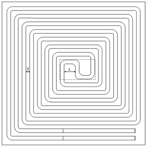
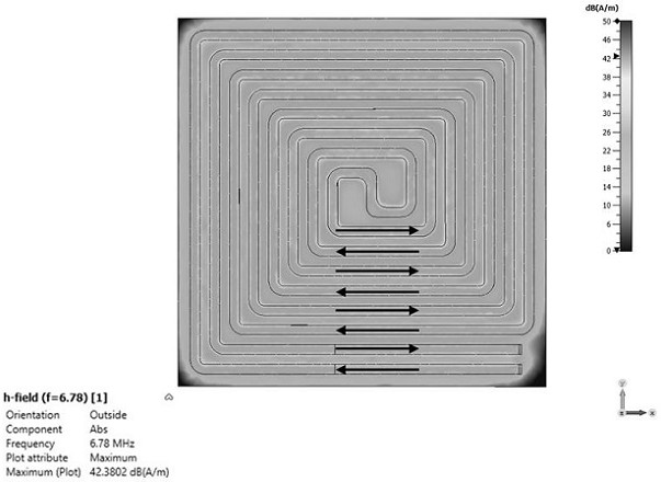
[0037] A short-distance one-to-many wireless charging device, including a transmitting coil. The transmitting coil is a single metal wire wound from the outside to the inside. It is similar to the pattern pattern of "wealth and wealth do not reach the end"; this kind of circuit enters in one line and exits in the same line, so that the current direction of each turn and adjacent turns is opposite, such as Figure 1-2 shown.
[0038] The transmitting coil is set on the substrate, and one line is presented coherently at one time. The entire large substrate is a coil loop, unlike Qi’s that each coil passes through a layer of Litz wire, a layer of glue, and a layer of magnetic chips. A layer of plastic or metal compartments and so on stacked up.
[0039] In some embodiments, figure 1 The central short-circuit area of the middle coil is symmetrical about the center of the coil, and the surrounding magnetic field is averaged, and the central short-circuit area is shown in figur...
Embodiment 2
[0043] The surface of the substrate is covered with a metal layer, because the magnetic field is all from the single-sided copper-clad substrate (copper-clad laminate), so the magnetic field passing through the substrate is less, which reduces the influence of the tangential loss of the substrate on the transmission efficiency of the wireless charging device. The thickness of the copper layer is 1-5 ounces (OZ). In some embodiments, the substrate is FR-4 or PCB, both of which can realize high-efficiency power transmission; the surface of the substrate is covered with a metal layer. In some embodiments, the copper clad laminate does not use a solder mask; higher performance can be obtained by immersion silver.
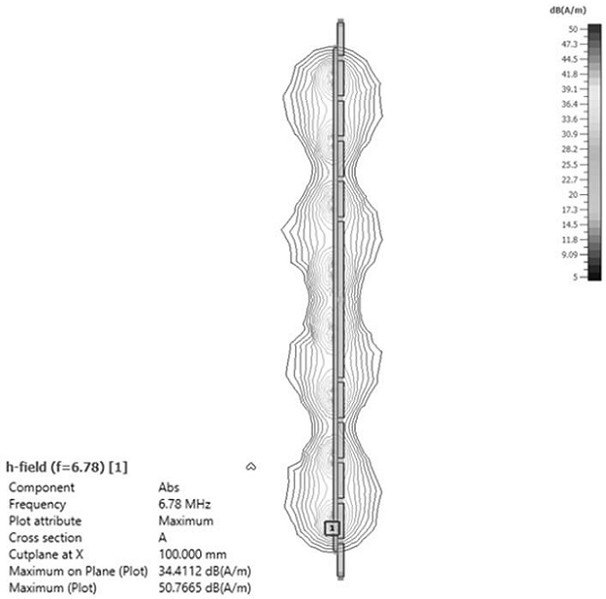
[0044] Embodiment 2 The simulated magnetic field of the wireless charging device whose substrate is a copper clad laminate, such as Figure 4 (Standard positive center cross-section), the black line on the right side of the figure is the metal layer, which separates th...
Embodiment 3
[0047] structured as Figure 9 Shown, the structure of embodiment 3 and embodiment 1,2 is similar, Figure 9 The distance between adjacent coils with opposite medium current direction is 8mm, the line width is 4mm, and the number of turns of the coil wound from outside to inside is 3; the simulation results are as follows Figure 10 (section of the vertical line on the right) as shown, with image 3 , Figure 4 Compared with the simulation results of Figure 10 The magnetic field distribution at the middle edge is smoother.
PUM
| Property | Measurement | Unit |
|---|---|---|
| width | aaaaa | aaaaa |
| width | aaaaa | aaaaa |
Abstract
Description
Claims
Application Information


