Chip output short circuit protection circuit
An output short circuit and circuit protection technology, applied in the field of circuits, can solve the problems of power tube damage, burning overvoltage and overcurrent protection chips, power tube voltage difference, etc.
- Summary
- Abstract
- Description
- Claims
- Application Information
AI Technical Summary
Problems solved by technology
Method used
Image

Examples
Embodiment 1
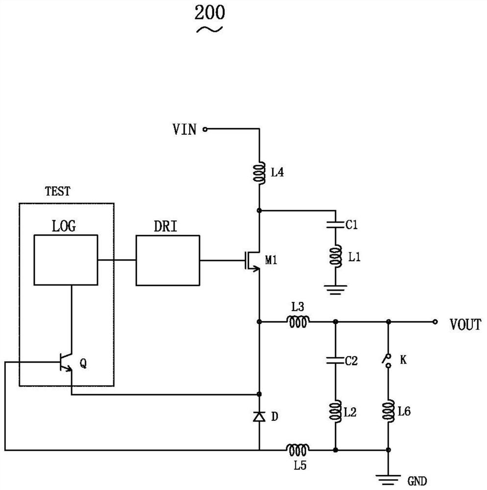
[0055] Please refer to image 3 As shown, the first embodiment provides a chip output short circuit protection circuit 200 . The detection module TEST in the chip output short-circuit protection circuit 200 in the first embodiment includes an NPN transistor Q and a logic module LOG.
[0056] Wherein, the logic module LOG is configured to control the driving module DRI to drive the first transistor M1 to turn on when it is determined that the voltage at the negative terminal of the diode D is negative.
[0057] In this implementation manner, the logic module LOG is an analog circuit. Of course, it is not limited thereto, and the logic module LOG may also be a digital-analog hybrid circuit or a digital circuit.
[0058] The specific circuit connection structure is: the collector of the NPN transistor Q is connected to the input terminal of the logic module LOG, the base of the NPN transistor Q is used as the second end of the detection module TEST, and the emitter of the NPN t...
Embodiment 2
[0062] Please refer to Figure 4 As shown, the second embodiment provides a chip output short circuit protection circuit 300 . The circuit in the chip output short-circuit protection circuit 300 in the second embodiment is basically the same as that in the first embodiment. The difference between the two embodiments is: the detection module TEST is an NMOS transistor M2. The NMOS transistor M2 detects whether the voltage at the negative terminal of the diode D is negative to directly trigger the driving module DRI. The NMOS transistor M2 can directly trigger the driving module DRI without setting the logic module LOG in the first embodiment, and the circuit is simpler.
[0063] The specific circuit connection structure is: the drain of the NMOS transistor M2 is used as the first terminal of the detection module TEST, the gate of the NMOS transistor M2 is used as the second terminal of the detection module TEST, and the source of the NMOS transistor M2 is used as the first te...
Embodiment 3
[0067] Please refer to Figure 5 As shown, the third embodiment provides a chip output short circuit protection circuit 400 . The circuit in the chip output short-circuit protection circuit 300 in the third embodiment is basically the same as that in the second embodiment. The difference between the two embodiments is: the chip output short-circuit protection circuit 400 in the third embodiment adds a third capacitor C3 on the basis of the second embodiment.
[0068] The first end of the third capacitor C3 is respectively connected to the output end of the driving module DRI and the gate of the first transistor M1; the second end of the third capacitor C3 is respectively connected to the first transistor The drain of M1, the second terminal of the fourth inductor L4, and the first terminal of the first capacitor C1.
[0069] The third capacitor C3 is the capacitance added by the gate-drain capacitive coupling of the first transistor M1. Its function is that during the rapid...
PUM
 Abstract
Description
Claims
Application Information
 - R&D
- Intellectual Property
- Life Sciences
- Materials
- Tech Scout
- Unparalleled Data Quality
- Higher Quality Content
- 60% Fewer Hallucinations
Browse by: Latest US Patents, China's latest patents, Technical Efficacy Thesaurus, Application Domain, Technology Topic, Popular Technical Reports.
© 2025 PatSnap. All rights reserved.Legal|Privacy policy|Modern Slavery Act Transparency Statement|Sitemap|About US| Contact US: help@patsnap.com