

Tri-state spintronic device, memory cell, memory array and read-write circuit
A spintronic device, spin-orbit coupling technology, applied in static memory, information storage, digital memory information and other directions, can solve problems such as increasing operations, achieve high reliability and circuit compatibility, and reduce the effect of memory area
- Summary
- Abstract
- Description
- Claims
- Application Information
AI Technical Summary
Problems solved by technology
Method used
Image


Examples
Embodiment Construction
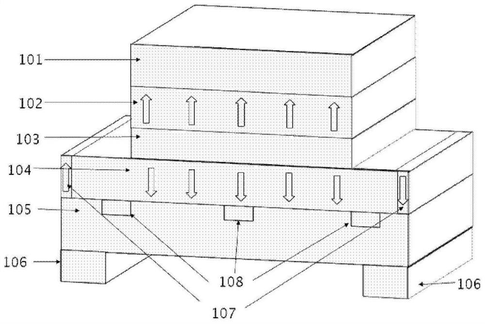
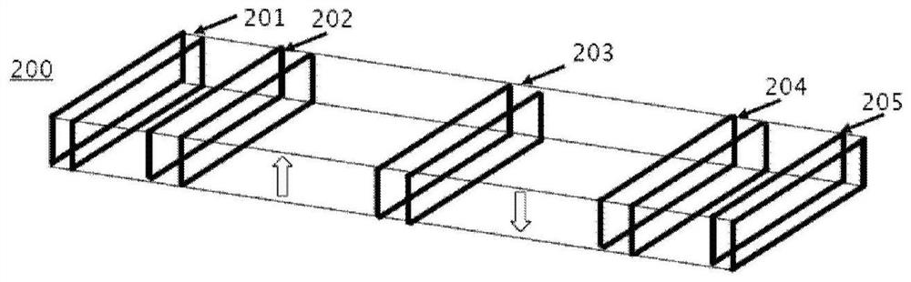
[0071] The present disclosure provides a three-state spintronic device, a storage unit, a storage array and a read-write circuit. The three-state spintronic device includes from bottom to top: a bottom electrode, a magnetic tunnel junction and a top electrode; a magnetic tunnel junction Including: spin-orbit coupling layer, ferromagnetic free layer, barrier tunneling layer and ferromagnetic reference layer, three local magnetic domain wall pinning centers and magnetic domain wall nucleation center; local magnetic domain wall pinning center Embedded in the spin-orbit coupling layer and in contact with the ferromagnetic free layer; the nucleation center of the magnetic domain wall is set at both ends of the ferromagnetic free layer; the current pulse is injected into the spin-orbit coupling layer to generate spin current to drive the ferromagnetic The magnetic domain walls in the free layer move and switch the resistive state. The present disclosure can effectively drive the mov...
PUM
 Abstract
Description
Claims
Application Information