Manufacturing method of intermediate isolation oxide layer of low-capacitance split-gate trench IGBT device

A technology for isolating oxide layers and intermediate isolation, which is applied in semiconductor/solid-state device manufacturing, electrical components, semiconductor devices, etc., and can solve problems such as insufficient breakdown voltage and reduced service quality of split-gate trench IGBT devices

Active Publication Date: 2021-05-14
JIANGSU HAIDONG SEMICON TECH CO LTD
View PDF6 Cites 0 Cited by
  • Summary
  • Abstract
  • Description
  • Claims
  • Application Information

AI Technical Summary

Problems solved by technology

[0004] The above-mentioned patent also has the following disadvantages: the breakdown voltage between the em

Method used


Image

  • Manufacturing method of intermediate isolation oxide layer of low-capacitance split-gate trench IGBT device
  • Manufacturing method of intermediate isolation oxide layer of low-capacitance split-gate trench IGBT device

Examples


Embodiment 1

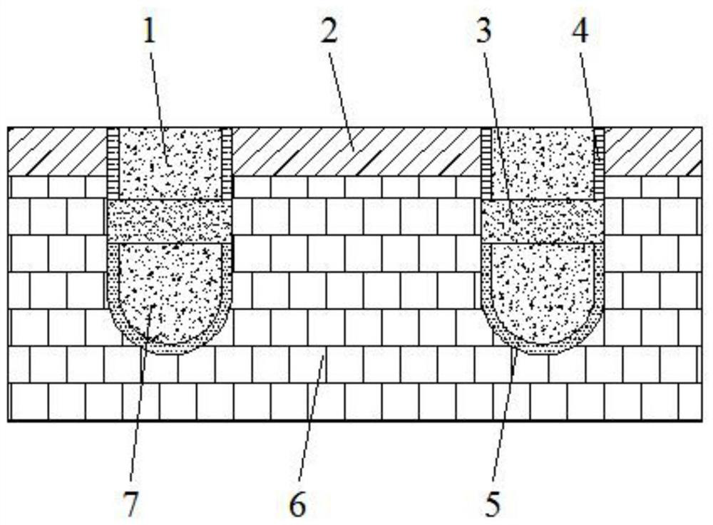
[0028] refer to Figure 1-2 , a fabrication of an isolation oxide layer in the middle of a low-capacity split-gate trench IGBT device, including an isolation oxide layer 3, a P well 2 and a silicon substrate 6, the P well 2 is arranged on the top of the silicon substrate 6, and the top of the P well 2 is opened There is a groove, the groove runs through the P well 2 and passes through the top of the silicon substrate 6, the gate oxide 4 is vertically arranged around the top of the groove, the gate polysilicon 1 is arranged inside the gate oxide 4, and the bottom thick oxide layer is arranged at the bottom of the groove. 5. The emitter polysilicon 7 is arranged inside the bottom thick oxide 5 , and the isolation oxide layer 3 is located between the gate polysilicon 1 and the emitter polysilicon 7 .

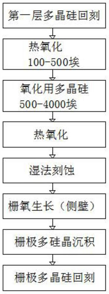
[0029] In the present invention, the isolation oxide layer 3 is obtained by combining thin oxygen plus polysilicon oxidation process.

[0030] In the present invention, the isolat...

Embodiment 2

[0040] refer to Figure 1-2 , a fabrication of an intermediate isolation oxide layer for a low-capacity divided gate trench IGBT device, comprising an isolation oxide layer 3, a P well 2 and a silicon substrate 6, the P well 2 is arranged on the top of the silicon substrate 6, and the P well 2 A groove is opened on the top, the groove runs through the P well 2 and passes through the top of the silicon substrate 6, and the gate oxide 4 is vertically arranged around the top of the groove, the gate polysilicon 1 is arranged inside the gate oxide 4, and the bottom of the groove is arranged There is a bottom thick oxide 5 , the emitter polysilicon 7 is arranged inside the bottom thick oxide 5 , and the isolation oxide layer 3 is located between the gate polysilicon 1 and the emitter polysilicon 7 .

[0041] In the present invention, the isolation oxide layer 3 is obtained by combining thin oxygen plus polysilicon oxidation process.

[0042] In the present invention, the isolation ...

Embodiment 3

[0052] refer to Figure 1-2, a fabrication of an intermediate isolation oxide layer for a low-capacity split-gate trench IGBT device, including an isolation oxide layer 3, a P well 2 and a silicon substrate 6, the P well 2 is arranged on the top of the silicon substrate 6, and the P well 2 A groove is opened on the top, the groove runs through the P well 2 and passes through the top of the silicon substrate 6, and the gate oxide 4 is vertically arranged around the top of the groove, and the gate polysilicon 1 is arranged inside the gate oxide 4, and the bottom of the groove is arranged There is a bottom thick oxide 5 , the emitter polysilicon 7 is arranged inside the bottom thick oxide 5 , and the isolation oxide layer 3 is located between the gate polysilicon 1 and the emitter polysilicon 7 .

[0053] In the present invention, the isolation oxide layer 3 is obtained by combining thin oxygen plus polysilicon oxidation process.

[0054] In the present invention, the isolation ...


PUM


Abstract

The invention belongs to the technical field of split-gate trench IGBT devices, and particularly relates to a manufacturing method of an intermediate isolation oxide layer of a low-capacitance split-gate trench IGBT device. For solving the problem that the breakdown voltage between an emitting electrode and a grid electrode is not high enough, the low-capacitance split-gate trench IGBT device comprises an isolation oxide layer, a P well and a silicon substrate, the P well is arranged at the top of the silicon substrate, a trench is formed in the top of the P well, the trench penetrates through the P well and the top of the silicon substrate, gate oxide is vertically arranged around the top of the trench, gate polycrystalline silicon is arranged in the gate oxide, bottom thick oxide is arranged at the bottom of the trench, emitter polycrystalline silicon is arranged in the bottom thick oxide, and the isolation oxide layer is located between the gate polycrystalline silicon and the emitter polycrystalline silicon. The dielectric constant of the silicon dioxide obtained by adopting a polycrystalline silicon oxidation process is higher than that of a film layer obtained by HDP, so that the breakdown voltage between the emitting electrode and the grid electrode can be improved.

Description

technical field [0001] The invention relates to the technical field of split-gate trench IGBT devices, in particular to the manufacture of an intermediate isolation oxide layer of a low-capacity split-gate trench IGBT device. Background technique [0002] IGBT (Insulated Gate Bipolar Transistor), Insulated Gate Bipolar Transistor, is a composite fully-controlled voltage-driven power semiconductor device composed of BJT (Bipolar Transistor) and MOS (Insulated Gate Field Effect Transistor), with MOSFET The advantages of high input impedance and low conduction voltage drop of GTR. The saturation voltage of GTR is low, the carrying current density is large, but the driving current is large; the driving power of MOSFET is small, the switching speed is fast, but the conduction voltage drop is large, and the current carrying density is small. The IGBT combines the advantages of the above two devices, with low driving power and low saturation voltage. It is very suitable for the c...

Claims


Application Information

Patent Timeline
IPC IPC(8): H01L29/739H01L29/423H01L21/331
CPCH01L29/66348H01L29/7397H01L29/4236
Inventor 夏华忠黄传伟李健诸建周吕文生
Owner JIANGSU HAIDONG SEMICON TECH CO LTD
Why Eureka
Try Eureka