Semiconductor light-emitting element

A light-emitting element and semiconductor technology, which is applied in the direction of semiconductor devices, electrical components, circuits, etc., can solve the problems of uneven current expansion, affecting the uniformity of luminous brightness of semiconductor light-emitting elements, and poor current expansion effect of electrode extension strips, etc.

Active Publication Date: 2021-05-18
TIANJIN SANAN OPTOELECTRONICS
View PDF8 Cites 0 Cited by
  • Summary
  • Abstract
  • Description
  • Claims
  • Application Information

AI Technical Summary

Problems solved by technology

[0004] In the existing vertical structure, the current spreads through the electrodes and the electrode extension strips, and the end of the electrode extension strips tends to have a poor current expansion effect, resulting in uneven current expansion, which affects the uniformity of the luminous brightness of the semiconductor light-emitting element

Method used


Image

  • Semiconductor light-emitting element
  • Semiconductor light-emitting element
  • Semiconductor light-emitting element

Examples


Embodiment 1

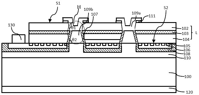
[0056] The present invention provides the following semiconductor light-emitting element, such as figure 1 The cross-sectional schematic diagram shown, which includes the following stacked layers: 100: substrate; L: semiconductor epitaxial stack; 102: first conductivity type semiconductor layer; 103: active layer; 104: second conductivity type semiconductor layer; 105: dielectric layer ; 106: second electrode metal layer; 107: side wall insulating layer; 108: second insulating layer; 109: electrical connection structure; 109a: the first section of the electrical connection structure; 109b: the first section of the electrical connection structure Second stage; 110: first electrode metal layer; 120: first electrode; 130: second electrode.

[0057] The details of each structural stack layer are described below.

[0058] The substrate 100 is a conductive substrate, and the conductive substrate can be silicon, silicon carbide, or a metal substrate, and the metal substrate is prefe...

Embodiment 2

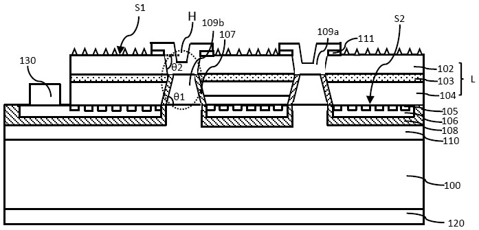
[0082] In this embodiment, if image 3 As shown, the difference from Example 1 is that the upper surface of the first conductive type semiconductor layer in Example 1 is smooth, and in the area covered by the static elimination connection structure in Example 2, the first conductive type semiconductor layer The remaining area of ​​the first surface of the first surface has a roughened structure. By roughening the remaining area of ​​the first surface of the first conductive type semiconductor layer, the light output of the semiconductor light emitting element can be increased, thereby improving the luminous efficiency of the semiconductor light emitting element.

Embodiment 3

[0084] In this embodiment, if Figure 4 As shown, the difference from Embodiment 1 is that the first section of the through hole in Embodiment 1 has a certain inclination angle, the first section of the through hole in Embodiment 3 is set to be vertical, and the first section of the through hole is vertical. Sections expose the first conductive type semiconductor layer 102. The segmented arrangement of the through holes is convenient for the operation of the manufacturing process, can reduce the aperture of the through holes, and reduce the area of ​​the sacrificed light-emitting region caused by digging holes, which can reduce the Luminance loss of the semiconductor light-emitting element; at the same time, the through-hole setting can improve the uniformity of current distribution, thereby improving the uniformity of luminous brightness and luminous efficiency of the semiconductor light-emitting element.


PUM

PropertyMeasurementUnit
Thicknessaaaaaaaaaa
Thicknessaaaaaaaaaa
Thicknessaaaaaaaaaa

Abstract

The invention discloses a semiconductor light emitting device. The element includes a semiconductor epitaxial stack having a first surface and a second surface opposite to the first surface and including a first conductive type semiconductor layer, a second conductive type semiconductor layer, and an active layer between the first conductive type semiconductor layer and the second conductive type semiconductor layer; a through hole penetrating at least the first conductive type semiconductor layer, the second conductive type semiconductor layer, and the active layer; a enlectrical connection structure, arranged in the through hole, extending to the first surface of the first conductive type semiconductor layer and electrically connected with the first conductive type semiconductor layer; a first electrode metal layer, arranged on the second surface of the semiconductor epitaxial laminated layer and connected with the electrical connection structure. The element is characterized in that at least one section of through hole is exposed out of the first conductive type semiconductor layer, the included angle between the side wall of the first section of through hole and the first surface is theta1, and theta1 is larger than 0 degree and smaller than or equal to 90 degrees. According to the invention, the uniformity of current expansion can be improved, and the uniformity of luminance and luminous efficiency of the semiconductor light-emitting element can be improved.

Description

technical field [0001] The invention relates to a semiconductor light-emitting element, which belongs to the field of semiconductor optoelectronic devices and technologies. Background technique [0002] Light Emitting Diode (English: Light Emitting Diode, referred to as: LED) is a semiconductor diode that can convert electrical energy into light energy. Compared with traditional electric lighting methods, LED lighting has the advantages of high luminous intensity, high efficiency, small size, and long service life. It is considered to be one of the most potential light sources at present. It is widely used in fields such as lights and large-screen displays. [0003] Existing light emitting diodes include horizontal types and vertical types. The vertical type light-emitting diode is obtained by transferring the semiconductor barrier stack to other substrates such as silicon, silicon carbide or metal substrates, and removing the original epitaxial growth substrate. Compared ...

Claims


Application Information

Patent Timeline
IPC IPC(8): H01L33/08H01L33/10
CPCH01L33/08H01L33/06H01L33/387H01L33/40H01L33/30H01L33/46H01L33/48H01L33/502H01L33/56H01L33/62H01L33/382H01L33/22H01L33/145
Inventor 张思于水利武晨明林坤德郭桓邵丘建生
Owner TIANJIN SANAN OPTOELECTRONICS
Why Eureka
Try Eureka