InP-based spot size converter and spot size conversion structure, and preparation methods thereof
A technology of mold spot converter and conversion structure, which is applied in the direction of light guide, optics, optical components, etc., and can solve the problems of increasing packaging cost and large size
- Summary
- Abstract
- Description
- Claims
- Application Information
AI Technical Summary
Problems solved by technology
Method used
Image

Examples
preparation example Construction
[0023]According to an embodiment of the present invention, a method for preparing the above-mentioned InP-based SSC is provided, including: sequentially forming two or more layers of In x Ga 1-x As y P 1-y layer to obtain a vertical tapered structure.
[0024] According to an embodiment of the present invention, the In x Ga 1-x As y P 1-y The layers are formed by metalorganic chemical vapor deposition. It is easier to prepare In by using the method of organometallic chemical vapor deposition x Ga 1-x As y P 1-y layer.
[0025] According to an embodiment of the present invention, a speckle conversion structure is provided, comprising: a substrate; an InP buffer layer formed on the substrate; x Ga 1-x As y P 1-y Layers and InP layers alternately arranged diluted waveguide layer, formed on the InP buffer layer; above-mentioned InP-based SSC, formed on the InP layer of the diluted waveguide (DW) layer; wherein, the InP-based SSC and DW In x Ga 1-x As y P 1-y La...
Embodiment 1
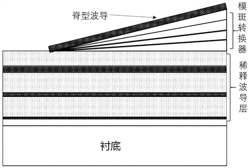
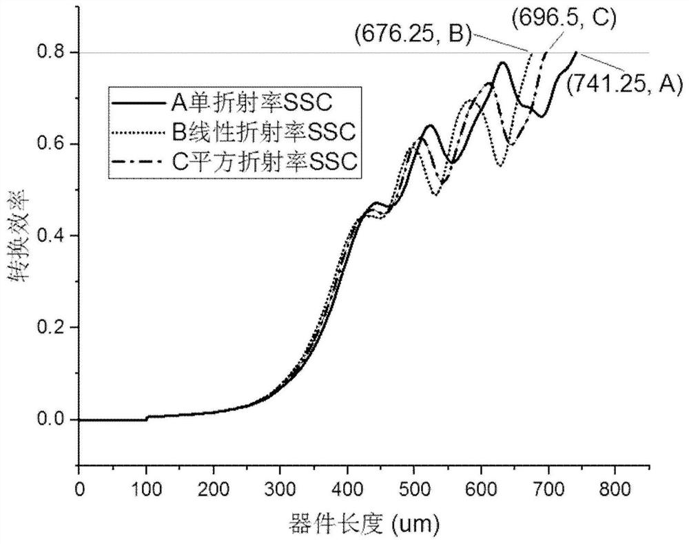
[0037] Such as Figures 1 to 3 As shown, a speckle conversion structure includes: InP substrate, InP buffer layer, DW layer, InP-based SSC and ridge waveguide from bottom to top, wherein, SSC is In x Ga 1-x As y P 1-y , each In x Ga 1-x As y P 1-y The layers from bottom to top are as follows: the peak Q of photoluminescence spectrum is 1.06, the thickness is 630nm, and the refractive index is n 1 =3.268; the photoluminescence spectrum peak Q is 1.15, the thickness is 210nm, and the refractive index is n 2 = 3.304. The peak Q of the photoluminescence spectrum of the ridge waveguide material is 1.06. In the 1550nm band, the numerical simulation of the light field speckle conversion efficiency is carried out for this speckle conversion structure, and the simulation results are as follows image 3 shown.
Embodiment 2
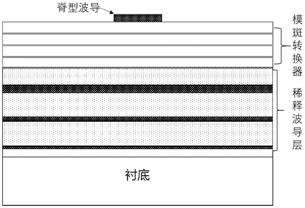
[0039] Such as Figures 1 to 3 As shown, a mode spot conversion structure, including from bottom to top: InP substrate, InP buffer layer, DW layer, InP-based SSC and ridge waveguide, wherein, SSC adopts three-layer refractive index square gradient to increase In x Ga 1-x As y P 1-y , from bottom to top, the peak Q of the photoluminescence spectrum is 1.06, the thickness is 630nm, and the refractive index is n 1 =3.268; the peak Q of the photoluminescence spectrum is 1.15, the thickness is 110nm, and the refractive index n 2 =3.304; the photoluminescence spectrum peak Q is 1.06, and the refractive index is n at a thickness of 100nm 1 = 3.268. The peak Q of the photoluminescence spectrum of the ridge waveguide material is 1.06. In the 1550nm band, the numerical simulation of the light field speckle conversion efficiency is carried out for this speckle conversion structure, and the simulation results are as follows image 3 shown.
[0040] After the entire mode spot conve...
PUM
| Property | Measurement | Unit |
|---|---|---|
| thickness | aaaaa | aaaaa |
| thickness | aaaaa | aaaaa |
| thickness | aaaaa | aaaaa |
Abstract
Description
Claims
Application Information
 - R&D Engineer
- R&D Manager
- IP Professional
- Industry Leading Data Capabilities
- Powerful AI technology
- Patent DNA Extraction
Browse by: Latest US Patents, China's latest patents, Technical Efficacy Thesaurus, Application Domain, Technology Topic.
© 2024 PatSnap. All rights reserved.Legal|Privacy policy|Modern Slavery Act Transparency Statement|Sitemap