
Semiconductor structure and forming method thereof

A semiconductor and conductive layer technology, applied in the field of semiconductor structure and its formation, can solve problems such as poor magnetic tunnel junction performance, and achieve the effect of good performance

Pending Publication Date: 2021-06-11
SEMICON MFG INT (SHANGHAI) CORP +1
View PDF0 Cites 0 Cited by
  • Summary
  • Abstract
  • Description
  • Claims
  • Application Information

AI Technical Summary

Problems solved by technology

[0004] However, the performance of the magnetic tunnel junction prepared by the prior art is poor

Method used


Image

  • Semiconductor structure and forming method thereof
  • Semiconductor structure and forming method thereof
  • Semiconductor structure and forming method thereof

Examples


Embodiment Construction

[0035] As mentioned in the background, existing semiconductor structures perform poorly.

[0036] The reasons for the poor performance of the semiconductor structure will be described in detail below in conjunction with the accompanying drawings. Figure 1 to Figure 4 A schematic diagram of a semiconductor structure.

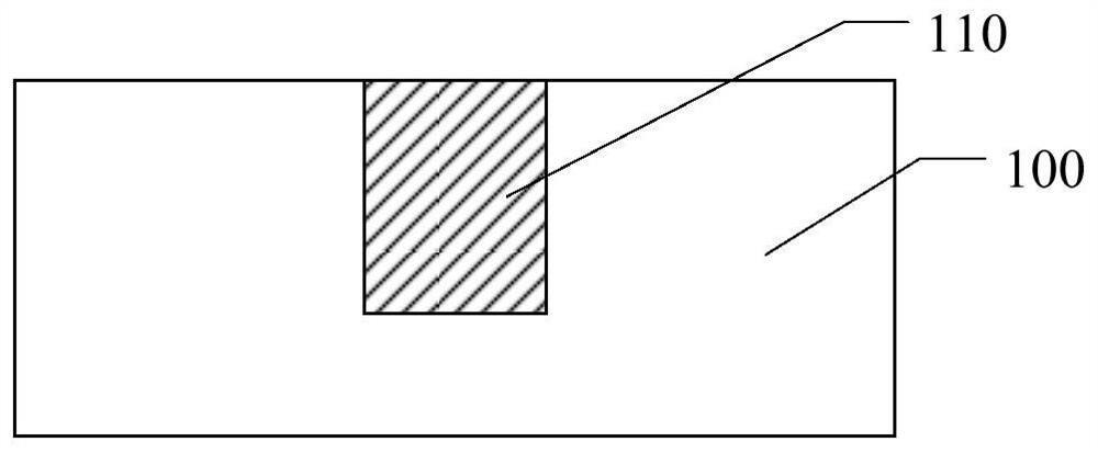
[0037] Please refer to figure 1 , providing a base 100, the base 100 has a conductive layer 110 inside, and the base 100 exposes the surface of the conductive layer 110.

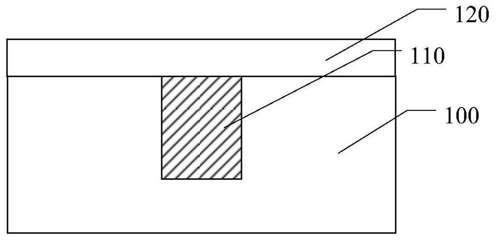
[0038] Please refer to figure 2 , forming an underlying electromagnetic material film 120 on the surface of the substrate 100 and the surface of the conductive layer 110 .

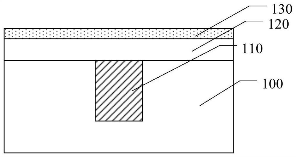
[0039] Please refer to image 3 , forming an insulating film 130 on the surface of the underlying electromagnetic material film 120 .

[0040] Please refer to Figure 4 , forming a top electromagnetic material film 140 on the surface of the insulating film 130 .

[0041] In the above method, a bottom layer electromag...


PUM

PropertyMeasurementUnit
Thicknessaaaaaaaaaa

Abstract

The invention discloses a semiconductor structure and a forming method thereof. The method comprises the steps of providing a substrate; forming a bottom electromagnetic material film on the surface of the substrate; forming a precursor film on the surface of the bottom electromagnetic material film; forming a first insulating film on the surface of the precursor film; carrying out annealing treatment to enable the precursor film to form a second insulating film; and forming a top electromagnetic material film on the surface of the first insulating film. The method can improve the performance of the formed semiconductor structure.

Description

technical field [0001] The invention relates to the technical field of semiconductor manufacturing, in particular to a semiconductor structure and a forming method thereof. Background technique [0002] MRAM (Magnetic Random Access Memory) is a non-volatile magnetic random access memory. It has the high-speed read and write capabilities of static random access memory (SRAM), high integration of dynamic random access memory (DRAM) and power consumption far lower than DRAM, compared with flash memory (Flash), with the use of time Increase performance without degradation. Due to the above-mentioned characteristics of MRAM, it is called universal memory and is considered to be able to replace SRAM, DRAM, EEPROM and Flash. [0003] Unlike traditional random access memory chip fabrication technology, data in MRAM is not stored in the form of charge or current, but in a magnetic state, and is sensed by measuring resistance without disturbing the magnetic state. MRAM uses a magne...

Claims


Application Information

Patent Timeline
IPC IPC(8): H01L43/12H01L43/08
CPCH10N50/01H10N50/10G11C11/161H01L29/82H10N50/80H10N50/85
Inventor 周鸣
Owner SEMICON MFG INT (SHANGHAI) CORP
Learn More