

Monolithic and system-level circuit integrated package structure of terahertz microstrip probe without jumper
A technology of microstrip probe and packaging structure, which is applied in the direction of circuits, connecting devices, electrical components, etc., can solve the problems of inability to guarantee repeatability and consistency, high transmission loss, etc., to save chip thinning process and reduce loss , to eliminate the effect of large discontinuities
- Summary
- Abstract
- Description
- Claims
- Application Information
AI Technical Summary
Problems solved by technology
Method used
Image

Examples
Embodiment Construction
[0037] In order to facilitate those skilled in the art to understand the technical content of the present invention, the content of the present invention will be further explained below with reference to the accompanying drawings.
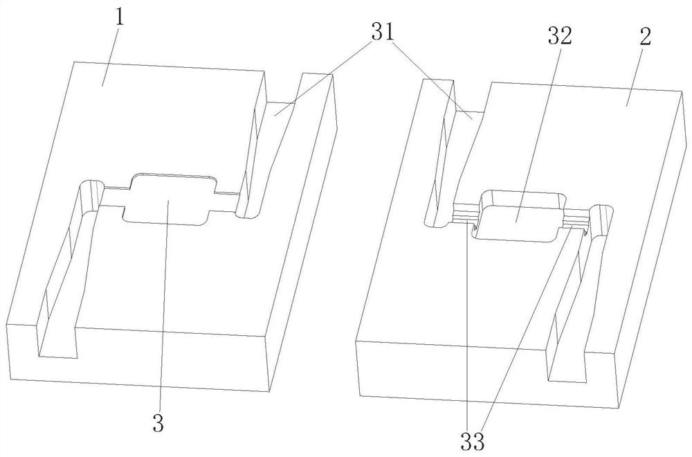
[0038] like figure 2 and image 3 As shown in the figure, the terahertz microstrip probe monolithic and system-level circuit interconnection integrated package in this embodiment includes a lower cavity 1, an upper cavity 2, a shielding cavity 3 formed between the upper and lower cavities, and The microstrip probe is interconnected and packaged in an integrated structure 4. The upper cavity 2 is assembled on the lower cavity 1 to form a rectangular waveguide cavity 31, a microstrip circuit shielding cavity 32 and a monolithic circuit shielding cavity 33.
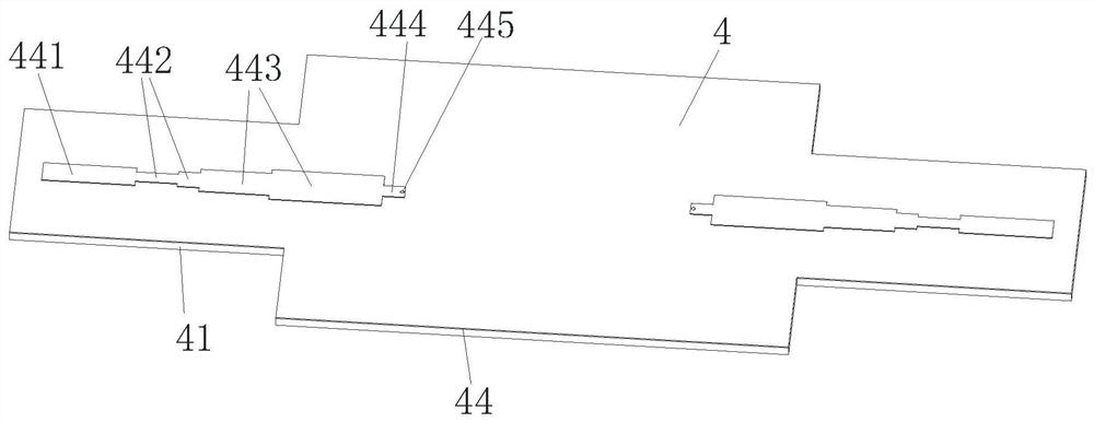
[0039] like image 3 , Figure 4 and Figure 5As shown, the microstrip probe interconnection package integrated structure 4 in this embodiment includes a microstrip probe 441, a probe impeda...
PUM
 Abstract
Description
Claims
Application Information