Terahertz jump-free coplanar waveguide monolithic and system-level circuit low insertion loss packaging structure

A technology of coplanar waveguide and packaging structure, applied in waveguides, circuits, waveguide-type devices, etc., can solve the problem of inability to use terahertz monolithic and system-level circuit packaging structures on a large scale, easy fracture of quartz substrates, and complex processing technology. problem, to achieve the effect of eliminating chip thinning process, eliminating metal stripping, and low transmission insertion loss

Active Publication Date: 2022-05-03
UNIV OF ELECTRONICS SCI & TECH OF CHINA
View PDF3 Cites 0 Cited by
  • Summary
  • Abstract
  • Description
  • Claims
  • Application Information

AI Technical Summary

Problems solved by technology

At present, there are very limited methods to reduce the dielectric loss in the terahertz frequency band. The common method is to use quartz as the substrate of the planar transmission line. The quartz substrate has relatively small dielectric loss, but the quartz substrate is easy to break, the processing technology is complicated, and the cost is high. Factors, cannot be used in large-scale terahertz monolithic and system-level circuit packaging structures

Method used


Image

  • Terahertz jump-free coplanar waveguide monolithic and system-level circuit low insertion loss packaging structure
  • Terahertz jump-free coplanar waveguide monolithic and system-level circuit low insertion loss packaging structure
  • Terahertz jump-free coplanar waveguide monolithic and system-level circuit low insertion loss packaging structure

Examples


Embodiment Construction

[0040] In order to make the object, technical solution and advantages of the present invention clearer, the present invention will be further described in detail below in conjunction with the accompanying drawings and embodiments. It should be understood that the specific embodiments described here are only used to explain the present invention, not to limit the present invention.

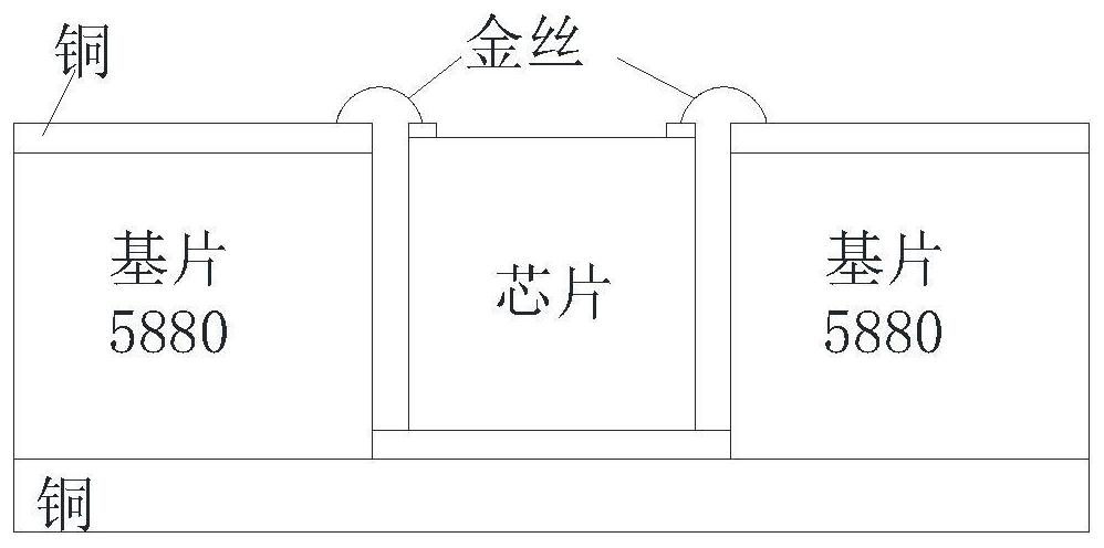
[0041] The coplanar waveguide transmission line uses metal atom sputtering technology to make high-precision metal patterns on the Pi dielectric layer. The center is the signal transmission line, and the metal ground planes are symmetrically distributed on both sides. The plastic sealing layer and the Pi dielectric layer constitute a double-layer composite dielectric substrate, in which the thickness of the plastic sealing layer is 150-200um (because the thickness of the plastic sealing layer is greater than 150um, it is easy to process, if it is consistent with the thickness of the terahertz chip, ...


PUM


Abstract

The invention discloses a terahertz jumper-free coplanar waveguide monolith and a system-level circuit low-insertion-loss packaging structure, which is applied to the technical field of circuit packaging. The problem is that the present invention punches holes in the Pi dielectric layer above each chip test pad to make a hole-shaped interconnection structure, so that the test pad is connected to the coplanar waveguide microstrip without the need of the traditional gold wire bonding jumper structure, and the microstrip is matched with the interconnection The branch connection is used to correct the impedance mismatch introduced by the hole-shaped interconnection structure. Since the hole-shaped interconnection structure and the interconnection matching branches are made by high-precision metal atom sputtering technology, good consistency and repeatability can be guaranteed.

Description

technical field [0001] The invention belongs to the technical field of circuit packaging, and in particular relates to a terahertz device packaging technology. Background technique [0002] In a broad sense, terahertz waves refer to electromagnetic waves with frequencies ranging from 100GHz to 10THz (corresponding to a wavelength of 3mm to 30um). Since terahertz waves are located in the transition zone between macroelectronics and microphotonics, they have many unique properties. Compared with microwave and millimeter waves, terahertz waves have the characteristics of high frequency and short wavelength. Therefore, terahertz waves have stronger beam directionality, higher resolution, and greater information capacity, and electronic devices can be made smaller. Compared with light waves, terahertz waves have stronger penetrability, can be applied to environments such as rain, fog, and smoke-filled battlefields, and have the ability to work around the clock; terahertz waves ha...

Claims


Application Information

Patent Timeline
Patent Type & Authority Patents(China)
IPC IPC(8): H01P3/00H01P3/10H01P3/12H01P3/16
CPCH01P3/00H01P3/12H01P3/10H01P3/16
Inventor 王志刚余波王俊辉延波
Owner UNIV OF ELECTRONICS SCI & TECH OF CHINA
Why Eureka
Try Eureka