Electronic industry-oriented circuit board identification and bonding pad/chip rapid positioning method

A technology in the electronics industry and a positioning method, which is applied in image data processing, instruments, calculations, etc., can solve problems such as being susceptible to external environmental interference, low positioning efficiency, and dense target points, so as to achieve low external environmental interference, excellent recognition rate, Create simple effects

Pending Publication Date: 2021-06-25
SHENYANG INST OF AUTOMATION - CHINESE ACAD OF SCI
View PDF0 Cites 1 Cited by
  • Summary
  • Abstract
  • Description
  • Claims
  • Application Information

AI Technical Summary

Problems solved by technology

[0003] The invention is closely related to the actual needs, and aims at the problems of robot visual guidance and fast and precise positioning, adopts the modeling and matching algorithm based on the multi-layer contour feature model, realizes the rapid identification and classification of various printed circuit boards, and aims at the existing methods Due to the problems of low positioning efficiency, dense target points and susceptibility to external environment interference, a modeling and matching algorithm based on the multi-layer deformable component model is proposed, which realizes the rapid and precise positioning of the target solder joint group of the printed circuit board, and the fitting Multi-target center coordinates, the position information of the pad and chipset is transmitted to the robot control and motion execution system, so as to realize the attachment, assembly, sorting, grinding, dispensing, testing, Welding and other processes provide the necessary key technologies

Method used


Image

  • Electronic industry-oriented circuit board identification and bonding pad/chip rapid positioning method
  • Electronic industry-oriented circuit board identification and bonding pad/chip rapid positioning method
  • Electronic industry-oriented circuit board identification and bonding pad/chip rapid positioning method

Examples


Embodiment Construction

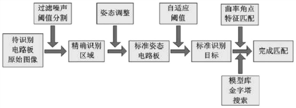
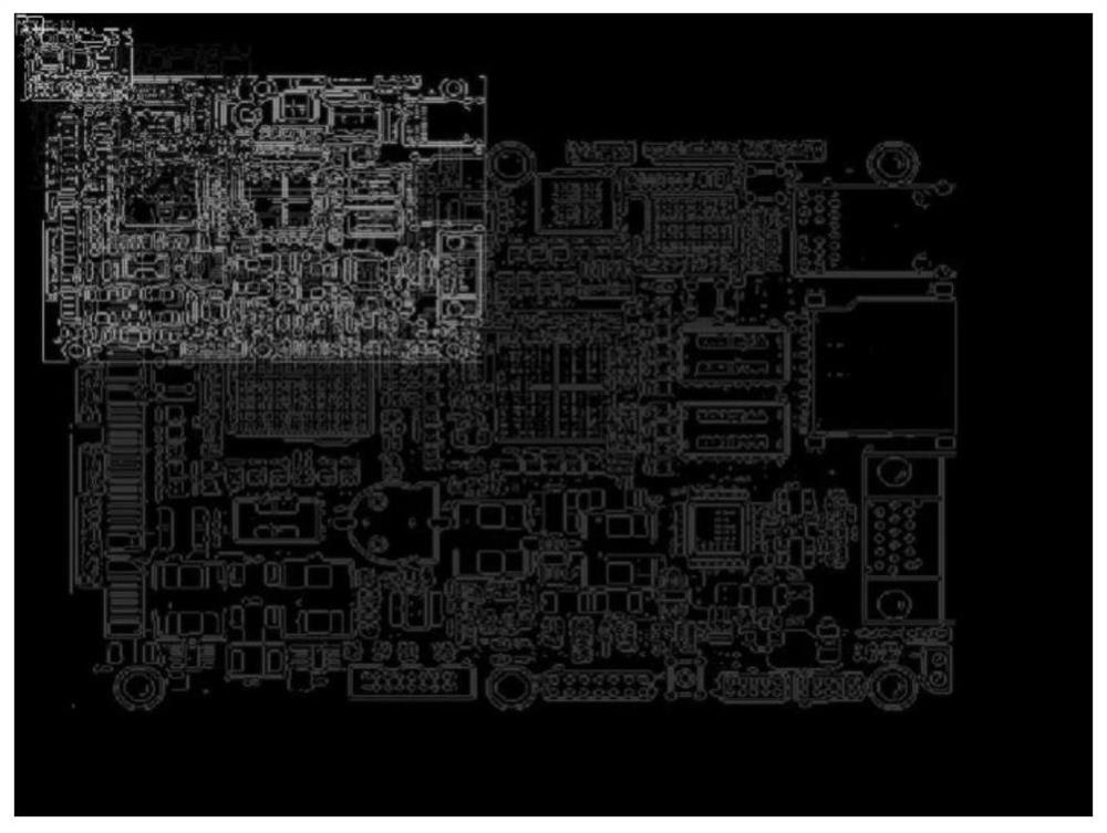
[0045] The specific functional objectives of the present invention can be divided into two parts: one is to realize the rapid identification and classification of various printed circuit boards, and establish a standard identification library, so that the identification success rate is higher than 99%; The position information of the pads of the circuit board or the chipset, so as to realize the fast and precise positioning of the measured target, and ensure that the algorithm efficiency is better than 200ms.

[0046] The present invention will be further described in detail below in conjunction with the accompanying drawings and embodiments.

[0047] The technical solution of the present invention is divided into two parts: one is the rapid identification and classification technology of multi-type printed circuit boards under the free posture;

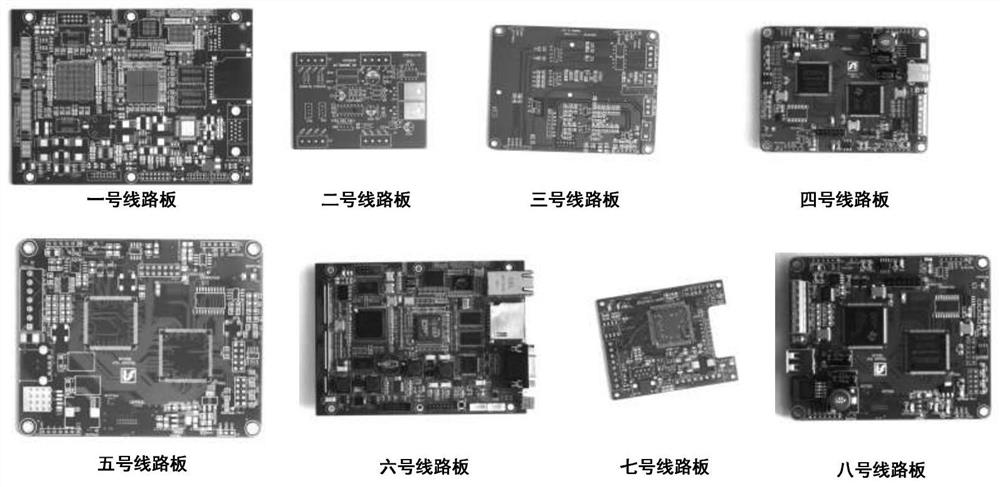
[0048] 1. Rapid identification and classification technology of multi-type printed circuit boards in free posture

[0049] The cor...


PUM


Abstract

The invention belongs to the field of the electronic industry, and particularly relates to a circuit board identification and bonding pad/chip precise and rapid positioning method. The method comprises the following steps: carrying out noise filtering and threshold segmentation on a to-be-recognized original image to obtain an ROI (Region of Interest); performing affine transformation on the ROI to obtain an image of a horizontal attitude; carrying out adaptive threshold processing on the image of the horizontal attitude to obtain a recognition target; and carrying out deformable component image matching (DPM) based on contour curvature angular point features and pyramid model search on the identified target and the model database, and completing matching, namely completing rapid positioning of the chip. According to the invention, rapid identification and classification of various printed circuit boards can be realized. According to the method, the area position of the bonding pad group point can be accurately positioned, the robustness is high, the adverse influence of the bonding pad or the chip group area due to image deformation can be overcome, and the algorithm execution efficiency is high. The method can meet the special requirements of intelligent mistake and omission prevention, mixed line production of circuit boards and the like in the electronic industry.

Description

technical field [0001] The invention is oriented to the field of electronics industry, and specifically relates to a circuit board identification and pad / chip precise and fast positioning method. Background technique [0002] At present, there are four common problems in the demand side of the electronic manufacturing industry in the parts manufacturing and assembly process: labor-intensive automation, high labor costs, difficulty in recruiting people, complex processes and fast replacement, low labor efficiency and yield, and short delivery times. Machine vision is an important part of the research in the field of collaborative small assembly robots, especially the technology of circuit board recognition and pad / chip rapid positioning, which is the key to realizing small batch customization, personalized manufacturing and flexible manufacturing in the electronics manufacturing industry. In the field of machine vision research, object recognition by analyzing images is an im...

Claims


Application Information

Patent Timeline
Patent Type & Authority Applications(China)
IPC IPC(8): G06T7/00G06T5/00G06T3/00G06T7/12G06T7/136G06T7/73
CPCG06T3/0006G06T5/002G06T7/0004G06T2207/10004G06T2207/30148G06T7/12G06T7/136G06T7/73
Inventor 李兴强杜劲松白珈郡丛日刚褚云凯
Owner SHENYANG INST OF AUTOMATION - CHINESE ACAD OF SCI
Why Eureka
Try Eureka