Switching current integrator for high power density buck switching converter
A switching converter, high power density technology, applied in the direction of electronic switches, high-efficiency power electronic conversion, electrical components, etc., can solve problems such as poor transient response, achieve the effect of reducing chip area and improving low-frequency gain
- Summary
- Abstract
- Description
- Claims
- Application Information
AI Technical Summary
Problems solved by technology
Method used
Image
Examples
Embodiment Construction
[0040] The specific embodiment of the present invention is described below in conjunction with accompanying drawing:
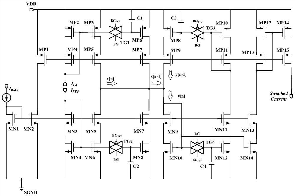
[0041] The specific circuit of the switching current integrator used in the high power density step-down switching converter of the present invention is as follows image 3 shown, including the first capacitor C 1 , the second capacitance C 2 , the third capacitor C 3 , the fourth capacitor C 4 , the first transmission gate TG 1 , the second transmission gate TG 2 , the third transmission gate TG 3 , the fourth transmission gate TG 4 , the first NMOS transistor MN1, the second NMOS transistor MN2, the third NMOS transistor MN3, the fourth NMOS transistor MN4, the fifth NMOS transistor MN5, the sixth NMOS transistor MN6, the seventh NMOS transistor MN7, the eighth NMOS transistor MN8, the The ninth NMOS transistor MN9, the tenth NMOS transistor MN10, the eleventh NMOS transistor MN11, the twelfth NMOS transistor MN12, the thirteenth NMOS transistor MN13,...
PUM
 Abstract
Description
Claims
Application Information


