Epitaxial structure of blue-green light chip for phototherapy and preparation method thereof
An epitaxial structure, blue-green light technology, applied in the direction of phototherapy, semiconductor devices, electrical components, etc., can solve the problems that are not conducive to improving the effective radiation intensity of phototherapy instruments
- Summary
- Abstract
- Description
- Claims
- Application Information
AI Technical Summary
Problems solved by technology
Method used
Image
Examples
Embodiment 1
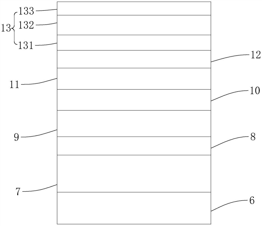
[0056] refer to figure 2 , an epitaxial structure of a blue-green light chip for phototherapy, prepared according to the following steps:
[0057] (1) Using MOCVD equipment, under the conditions of 1050°C and 75Torr, a 41nm thick GaN layer and a 43nm thick GaAlN layer are alternately deposited on the substrate 6, and a GaN layer and a GaAlN layer constitute a pair of III-V group compounds Layer, after the deposition of the III-V group compound layer is completed, the reflective DBR layer 7 is obtained, wherein the substrate 6 is a sapphire substrate, and the doping concentration of the reflective DBR layer 7 is 0;
[0058] (2) Under the conditions of 1050°C and 75Torr, deposit a doping concentration of 1E19cm on the reflective DBR layer 7 -3 n-type GaN to obtain a first n-type GaN layer 8 with a thickness of 2000nm;
[0059] (3) Under the conditions of 750° C. and 250 Torr, alternately deposit 3 nm thick quantum well layer InGaN and 4 nm thick quantum barrier layer GaN on t...
Embodiment 12-15
[0068] As shown in Table 2, the difference between Examples 12-15 and Example 10 lies in the different doping concentrations of the layers.
[0069] The doping concentration of the layer of table two embodiment 12-15
[0070]
Embodiment 16
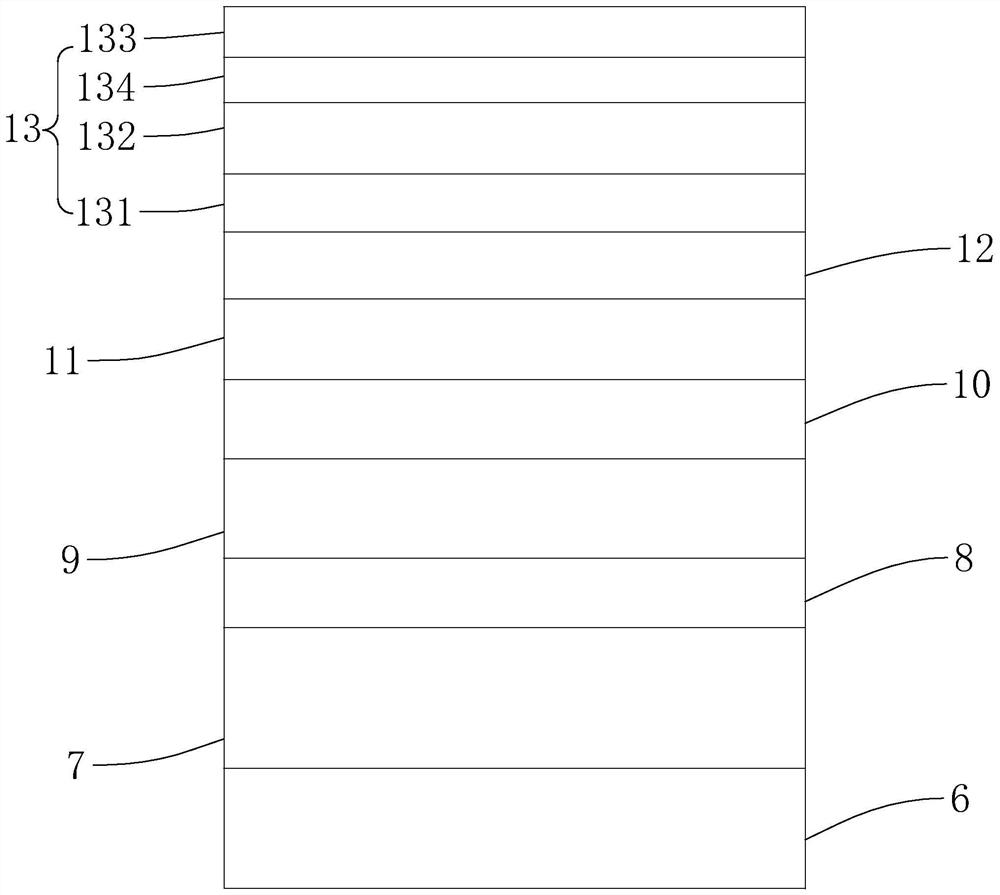
[0072] refer to image 3 , The difference between this embodiment and Embodiment 14 is that in step (8), firstly, under the conditions of 1075° C. and 75 Torr, a doping concentration of 1E20 cm is deposited on the second quantum well layer 132 -3 p-type AlGaN to obtain a p-type AlGaN layer 134 with a thickness of 70 nm; and then grow a second p-type GaN layer 133 on the p-type AlGaN layer 134 .
PUM
| Property | Measurement | Unit |
|---|---|---|
| thickness | aaaaa | aaaaa |
| beam angle | aaaaa | aaaaa |
| width | aaaaa | aaaaa |
Abstract
Description
Claims
Application Information


