Photonic crystal vertical cavity surface emitting laser

A vertical cavity surface emission, photonic crystal technology, applied in the field of optoelectronics, can solve the problems of thermal lens, poor stability, weakened control effect of photonic crystal structure, etc. The effect of far-field divergence

Active Publication Date: 2021-07-20
INST OF SEMICONDUCTORS - CHINESE ACAD OF SCI
View PDF6 Cites 5 Cited by
  • Summary
  • Abstract
  • Description
  • Claims
  • Application Information

AI Technical Summary

Problems solved by technology

The traditional vertical cavity surface emitting laser has a large lateral size, and the carrier distribution of the high current is not uniform, and there is a thermal lens phenomenon, which will cause multi-transverse mode lasing.
In related technologies, although the single-mode operation of the device can be realized by reducing the diameter of the oxidation-limited hole, it will bring problems such as increased series resistance, severe heat generation, and poor stability.
[0003] In the process of realizing the disclosed concept, the inventors found that a two-dimensional photonic crystal structure with a central defect is introduced into the upper DBR of the vertical cavity surface emitting laser, Although the two-dimensional photonic crystal air hole can be used to further control the light field, and then obtain single-mode lasing similar to photonic crystal fiber, but the duty cycle of the photonic crystal air hole is too small, which will cause the photonic crystal structure to have a negative effect on the lateral direction. The control effect of the mode is weakened, and it is easy to cause multi-transverse mode lasing

Method used


Image

  • Photonic crystal vertical cavity surface emitting laser
  • Photonic crystal vertical cavity surface emitting laser
  • Photonic crystal vertical cavity surface emitting laser

Examples


Embodiment Construction

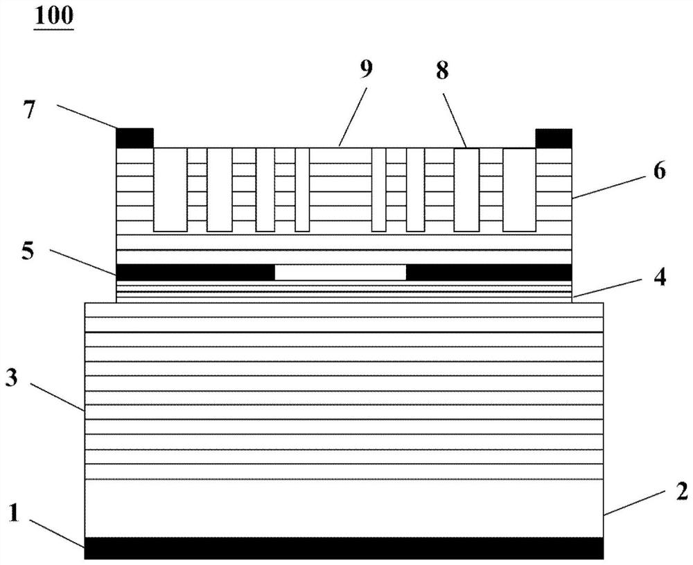
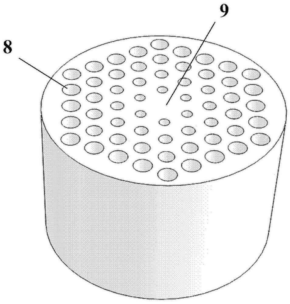
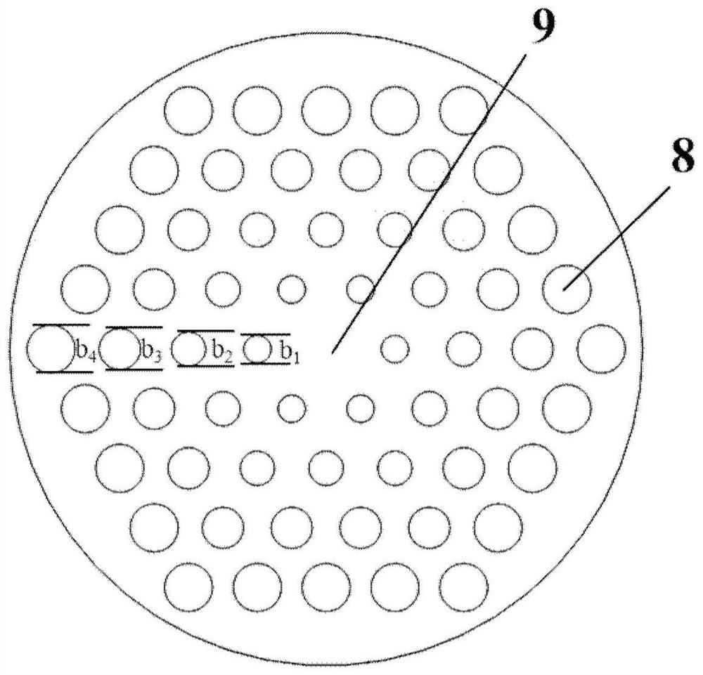
[0030] In order to make the purpose, technical solutions and advantages of the present disclosure clearer, the present disclosure will be further described in detail below in conjunction with specific embodiments and with reference to the accompanying drawings.

[0031] It should be noted that, in the drawings or descriptions of the specification, similar or identical parts all use the same figure numbers. Implementations not shown or described in the accompanying drawings are forms known to those of ordinary skill in the art. Additionally, while illustrations of parameters including particular values ​​may be provided herein, it should be understood that the parameters need not be exactly equal to the corresponding values, but rather may approximate the corresponding values ​​within acceptable error margins or design constraints. In addition, the directional terms mentioned in the following embodiments, such as "upper", "lower", "front", "rear", "left", "right", "inner", "out...


PUM

PropertyMeasurementUnit
thicknessaaaaaaaaaa

Abstract

The invention provides a photonic crystal vertical-cavity surface-emitting laser, and the laser comprises an oxidation limiting layer; a P-type DBR reflecting layer grown on the oxidation limiting layer, wherein the P-type DBR reflecting layer is etched with a light-emitting region and multiple layers of aperture gradient photonic crystal air hole structures which are periodically arranged along the radial direction of the light-emitting region; the multi-layer aperture gradient photonic crystal air hole structure is a two-dimensional photonic crystal air hole structure with a central point defect. According to the photonic crystal vertical cavity surface emitting laser, high-power single-mode lasing can be achieved, gradient distribution of refractive indexes is introduced in the radial direction of a light emitting area, the far-field divergence angle can be further reduced, and the light beam quality is improved.

Description

technical field [0001] The disclosure relates to the field of optoelectronic technology, in particular to a photonic crystal vertical cavity surface emitting laser. Background technique [0002] Vertical Cavity Surface Emitting Laser (VCSEL) is a semiconductor laser whose light output direction is perpendicular to the substrate surface. Compared with other semiconductor lasers, it has small divergence angle, high coupling efficiency, low threshold current, dynamic single longitudinal mode lasing, and low cost. Low-level advantages are widely used in space optical communication, laser radar, and pump sources. The basic structure of a common oxidation-limited vertical cavity surface emitting laser is composed of upper and lower DBRs, an active region and an oxide layer in the middle, and the oxide holes can realize the control of the electric field and the optical field. The traditional vertical cavity surface emitting laser has a large lateral size, and the distribution of c...

Claims


Application Information

Patent Timeline
Patent Type & Authority Applications(China)
IPC IPC(8): H01S5/183H01S5/065
CPCH01S5/18316H01S5/18319H01S5/18327H01S5/0654
Inventor 潘智鹏李伟刘素平马骁宇
Owner INST OF SEMICONDUCTORS - CHINESE ACAD OF SCI
Why Eureka
Try Eureka