
Coating treatment process for protective paint on surface layers of printed PCBs

A PCB board and surface layer technology, which is applied in the field of protective paint coating treatment process on the surface of printed PCB boards, can solve the problems that the surface contour of the PCB board cannot be sprayed, cannot be fully sprayed, and the surface of the PCB board is coated with dead angles, etc., so as to improve oil coating The effect of dipping in oil quickly, increasing activity, and avoiding leakage of oil

Inactive Publication Date: 2021-07-23
田科新
View PDF1 Cites 2 Cited by
  • Summary
  • Abstract
  • Description
  • Claims
  • Application Information

AI Technical Summary

Problems solved by technology

[0007] In view of the problems in the prior art, the purpose of the present invention is to provide a coating process for the surface protective paint of printed PCB boards, which solves the problem that the coating of the protective paint on the surface of the PCB board is mainly carried out by spraying. Covering, coating by spraying is likely to cause the surface contour of the PCB board (in the groove or micropore) to be sprayed or not completely sprayed, resulting in the technical problem of dead angle positions when coating the surface of the PCB board

Method used


Image

  • Coating treatment process for protective paint on surface layers of printed PCBs
  • Coating treatment process for protective paint on surface layers of printed PCBs
  • Coating treatment process for protective paint on surface layers of printed PCBs

Examples


Embodiment Construction

[0045] In order to make the technical means, creative features, goals and effects achieved by the present invention easy to understand, the present invention will be further elaborated below in conjunction with specific drawings. It should be noted that, in the case of no conflict, the embodiments and Features in the embodiments can be combined with each other.

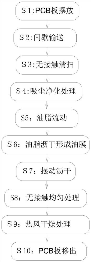
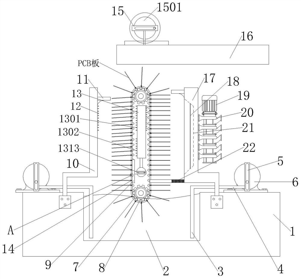
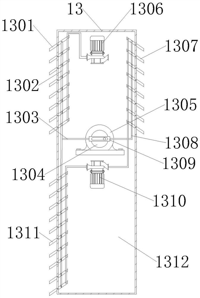
[0046] see Figure 1-5 It is a schematic diagram of the overall structure of the surface protection paint coating treatment process of a printed PCB board;

[0047] A kind of printed PCB board surface layer protective paint coating process is characterized in that, comprises the following steps:

[0048] S1. PCB board placement: place the PCB boards whose surface needs to be coated with grease upright on the automatic feeder, and install and fix each PCB board on the conveyor chain in an orderly manner through the automatic feeder, and the adjacent two PCB boards The distance between them is 10-15 cm;

[0049] S2. ...


PUM


Abstract

The invention provides a coating treatment process for protective paint on the surface layers of printed PCBs, and relates to the technical field of PCB production and processing. The coating treatment process comprises the following step of S1, PCB placement, wherein the PCBs with the surfaces needing to be coated with grease are vertically stacked on an automatic feeding machine, each PCB is mounted and fixed on a conveying chain through the automatic feeding machine in order, and the distance between every two adjacent PCBs ranges from 10 cm to 15 cm. According to the process, air blowing treatment is carried out on the surfaces of the PCBs before the PCBs are fed into an oil pool, dust adhering to the surfaces of the PCBs is swept away, in the sweeping process, the blown-out dust is adsorbed by a dust absorption device, floating of the dust in air can be effectively reduced, and by removing the dust on the surfaces of the PCBs, when the PCBs enter the oil pool to be dipped in oil, due to the fact that the surfaces of the PCBs are neat, the coating uniformity of the grease on the surfaces of the PCBs can be effectively improved.

Description

technical field [0001] The invention relates to the technical field of PCB board production and processing, in particular to a process for coating a protective paint on the surface of a printed PCB board. Background technique [0002] The Chinese name of PCB board is printed circuit board, also known as printed circuit board, which is an important electronic component, a support for electronic components, and a carrier for electrical interconnection of electronic components. Because it is produced using electronic printing, it is called a "printed" circuit board. [0003] At present, the surface of the PCB board has a layer of color, the common colors are green, blue, red and black, etc. In fact, these colors are a layer of oil film solidified on the PCB board after a layer of ink is dried. Commonly known as solder mask, the common solder mask is mainly applied by spraying, which is easy to exist [0004] At present, the patent number CN201821687807.7 discloses a PCB board...

Claims


Application Information

Patent Timeline
Patent Type & Authority Applications(China)
IPC IPC(8): B05D1/18B08B5/02B08B15/00B05C3/10B05C9/14B05C11/06B05C13/02B05D3/04H05K3/28
CPCB05C3/10B05C9/14B05C11/06B05C13/02B05D1/18B05D3/0406B05D3/0413B08B5/023B08B15/00H05K3/28
Inventor 田科新
Owner 田科新
Learn More